
An electrically driven on-chip integrated erbium-doped waveguide amplifier and its preparation method

A waveguide amplifier and electric drive technology, applied in the field of optoelectronics, can solve the problems of difficult realization of semiconductor amplifiers and unfavorable silicon-based integration, etc., and achieve the effect of low cost and simple process

Active Publication Date: 2021-12-10
PEKING UNIV
View PDF7 Cites 0 Cited by
  • Summary
  • Abstract
  • Description
  • Claims
  • Application Information

AI Technical Summary

Problems solved by technology

However, the material itself is difficult to epitaxially grow on a silicon substrate, which is not conducive to silicon-based integration; at the same time, limited by the band gap of the material, it is difficult to realize a III-V semiconductor amplifier in the 1.5μm band

Method used


Image

  • An electrically driven on-chip integrated erbium-doped waveguide amplifier and its preparation method
  • An electrically driven on-chip integrated erbium-doped waveguide amplifier and its preparation method
  • An electrically driven on-chip integrated erbium-doped waveguide amplifier and its preparation method

Examples


Embodiment Construction

[0040] In order to make the purpose, technical solutions and advantages of the embodiments of the present invention clearer, the technical solutions in the embodiments of the present invention will be clearly and completely described below in conjunction with the drawings in the embodiments of the present invention. Obviously, the described embodiments It is a part of embodiments of the present invention, but not all embodiments. Based on the embodiments of the present invention, all other embodiments obtained by persons of ordinary skill in the art without creative efforts fall within the protection scope of the present invention.

[0041] At present, on-chip amplification is a necessary technology in silicon-based optoelectronic chips, but reliable on-chip waveguide amplifiers are still not fully realized; although erbium-doped materials are recognized as suitable materials for optical amplifiers, erbium-doped optical waveguide amplifiers cannot be directly electrically pumpe...


PUM

PropertyMeasurementUnit
thicknessaaaaaaaaaa
widthaaaaaaaaaa
refractive indexaaaaaaaaaa

Abstract

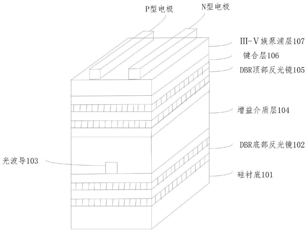
The embodiments of the present invention provide an electrically driven on-chip integrated erbium-doped waveguide amplifier and a preparation method thereof, including: a silicon substrate, a DBR bottom mirror, an optical waveguide, a gain medium layer, a DBR top mirror, Bonding layer, Ⅲ‑V group pump layer, Ⅲ‑V group pump layer generates pump light through electroluminescence, and indirectly electrically drives the gain medium layer in the intersecting direction of signal light transmission to generate amplification, Ⅲ‑V group semiconductor The light source is integrated into the bonding layer by epitaxial growth or patch bonding; the DBR bottom mirror and the DBR top mirror form a DBR resonant cavity to improve the pump power in the gain medium layer; the optical waveguide and the gain medium layer form a hybrid Waveguide structure. The invention adopts the III-V group semiconductor laser as the pump to realize electroluminescence; the III-V group semiconductor laser is integrated into the optical waveguide amplifier by means of growth or patch bonding, the process is simple and the cost is low.

Description

technical field [0001] The invention relates to the technical field of optoelectronics, in particular to an electrically driven on-chip integrated erbium-doped waveguide amplifier and a preparation method thereof. Background technique [0002] In recent years, microelectronics technology has developed rapidly according to Moore's law and has gradually become a bottleneck. Based on microelectronics technology, silicon-based optoelectronics technology that integrates optoelectronic devices on a chip has attracted more and more attention. It gives full play to the advantages of mature microelectronic technology, high integration, low cost, and low price, as well as the advantages of fast transmission rate, large bandwidth, and strong anti-interference ability of optical communication, and plays an increasingly important role in the field of communication. . On-chip optoelectronic devices, such as modulators, detectors, wavelength division multiplexers, etc., have gradually mat...

Claims


Application Information

Patent Timeline
Patent Type & Authority Patents(China)
IPC IPC(8): H01S5/125H01S5/04H01S5/30
CPCH01S5/125H01S5/041H01S5/305H01S5/3031H01S2304/00
Inventor 王兴军周佩奇王博何燕冬
Owner PEKING UNIV
Learn More