Method for directly preparing graphene on SiO2/Si substrate
A graphene and substrate technology, applied in the field of graphene preparation directly on SiO2/Si substrate, can solve problems such as inability to form graphene, achieve low cost, controllable number of layers, large-area growth, and high strength Effect
- Summary
- Abstract
- Description
- Claims
- Application Information
AI Technical Summary
Problems solved by technology
Method used
Image


Examples
preparation example Construction
[0029] figure 1 It simply shows the preparation process of the method of the present invention, which mainly includes three steps. The first step is based on the ion implantation method. 2 / Si substrate is implanted with carbon ions on the M film layer, after annealing treatment in the M / SiO 2 Graphene can be obtained on the upper and lower surfaces of the M film layer of the / Si substrate. Here M represents a transition metal layer. Whether graphene can be obtained on both the upper and lower surfaces of the M film layer depends on the thickness of the M film layer. Graphene can be obtained on both the upper and lower surfaces only when a suitable thickness of the M film layer is set. For each specific transition metal, the appropriate thickness can be obtained through a limited number of experiments.
[0030] The second step is to obtain direct deposition on SiO 2 The graphene on the surface of the / Si substrate needs to be removed from the graphene on the upper surface of the...
Embodiment 1
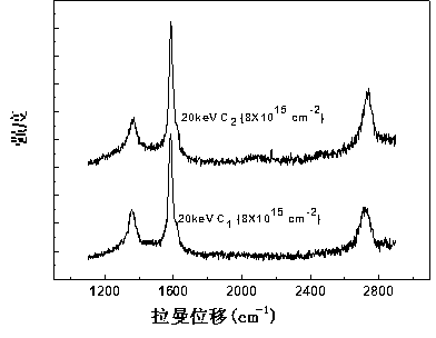
[0048] Under the condition of the suction voltage of 20keV, the beam intensity and XY scanning voltage of the ion implantation system were adjusted to obtain stable cluster carbon ions with the largest current intensity. Obtain C in this specific embodiment 1 And C 2 Cluster carbon ions, and C 1 And C 2 The cluster carbon ions were respectively implanted on the copper foil with a thickness of 25 μm, and the sample a and the sample b were obtained after annealing treatment. C 1 And C 2 The implantation dose of cluster carbon ions is 8×10 15 atoms / cm 2 , The injection energy is 20keV / atom and 10keV / atom respectively. The annealing process adopted in this embodiment is: keeping at 950°C for 30 minutes, and decreasing to room temperature at a rate of 20-30°C / min.
[0049] Use Raman spectroscopy to characterize samples a and b, see the results image 3 . It can be seen from the figure that the defect peak D of the graphene on sample a is at 1367cm -1 , The characteristic peak G, whic...
Embodiment 2
[0052] Under the condition of the suction voltage of 20keV, the cluster carbon ions are obtained by the ion implantation system, and the cluster carbon ions are implanted into Ni / SiO 2 / Si substrate nickel film surface, the implantation dose of cluster carbon ions is 4×10 16 atoms / cm 2 , Ni / SiO 2 The thickness of the nickel film in the / Si substrate is 300nm, SiO 2 The layer thickness is 300 nm. Ni / SiO for implanting cluster carbon ions 2 / Si substrate is annealed in Ni / SiO 2 To obtain graphene on the Ni film of the / Si substrate, the annealing process used is: hold at 900°C for 50 minutes, and drop to room temperature at a rate of 20°C / min. The Ni / SiO prepared with graphene obtained here 2 The / Si substrate is referred to as sample c for short. Use Raman spectroscopy to characterize sample c, and the obtained Raman spectra are shown in Figure 4 The spectral line in (1). It can be seen from the spectrum (1) that the intensity of the defect peak D peak is very small, and I D / ...
PUM
| Property | Measurement | Unit |
|---|---|---|
| thickness | aaaaa | aaaaa |
| thickness | aaaaa | aaaaa |
| thickness | aaaaa | aaaaa |
Abstract
Description
Claims
Application Information
 - R&D
- Intellectual Property
- Life Sciences
- Materials
- Tech Scout
- Unparalleled Data Quality
- Higher Quality Content
- 60% Fewer Hallucinations
Browse by: Latest US Patents, China's latest patents, Technical Efficacy Thesaurus, Application Domain, Technology Topic, Popular Technical Reports.
© 2025 PatSnap. All rights reserved.Legal|Privacy policy|Modern Slavery Act Transparency Statement|Sitemap|About US| Contact US: help@patsnap.com