
Chemical method for in-situ control and synthesis of AgCuS/Ag3CuS2 ternary semiconductor photoelectric thin-film material at normal temperature

A ternary compound, photoelectric thin film technology, applied in the field of material chemistry, can solve the problems of strong dependence on reaction vessels, inability to form films directly, complicated processes, etc., and achieve the effects of controllable film composition, convenient operation and simple reaction device

Active Publication Date: 2013-08-14
XUCHANG UNIV
View PDF3 Cites 3 Cited by
  • Summary
  • Abstract
  • Description
  • Claims
  • Application Information

AI Technical Summary

Problems solved by technology

[0005] The problem to be solved by the present invention is to overcome the disadvantages of strong dependence on the reaction vessel, high energy consumption, complex process, impure product, polluting the environment and inability to directly form a film in the current method for preparing sulfur-copper-silver ternary sulfide crystals.

Method used


Image

  • Chemical method for in-situ control and synthesis of AgCuS/Ag3CuS2 ternary semiconductor photoelectric thin-film material at normal temperature
  • Chemical method for in-situ control and synthesis of AgCuS/Ag3CuS2 ternary semiconductor photoelectric thin-film material at normal temperature
  • Chemical method for in-situ control and synthesis of AgCuS/Ag3CuS2 ternary semiconductor photoelectric thin-film material at normal temperature

Examples


Embodiment 1

[0041] 1. Preparatory work: The commercial ITO conductive glass is ultrasonically cleaned with detergent and deionized water for 20 minutes in sequence, and then the volume ratio of ammonia water (mass percentage: 25%): hydrogen peroxide (mass percentage: 30%): deionized water = 80 in the mixed solution of 1:2:5 o C boiled for 30min, and then ultrasonicated with deionized water for 20min again, and the cleaned ITO conductive glass was heated at 80 o C drying conditions. 40nm copper was first sputtered on the ITO surface by magnetron sputtering technology, and then 160nm silver was sputtered. Store the sample in a desiccator for later use;

[0042] 2. Reaction steps: Weigh 0.05g of sulfur powder and put it in a petri dish with a diameter of 100mm, add absolute ethanol, the amount is subject to the sample that can be submerged in step 1, and prepare the copper-silver metal layer prepared in step 1 The ITO conductive glass is placed flat in the petri dish to ensure that the sp...

Embodiment 2

[0045] 1, preparatory work: with embodiment 1.

[0046] 2. Reaction steps: Weigh 0.05g of sulfur powder and put it in a petri dish with a diameter of 100mm, add absolute ethanol, the amount is subject to the sample that can be submerged in step 1, and prepare the copper-silver metal layer prepared in step 1 Place the ITO conductive glass flat in the petri dish, ensure that the sputtered metal layer is upward, avoid direct contact with the sulfur powder, place the petri dish in a stable place, at 40 o Reaction under C conditions for 25 minutes;

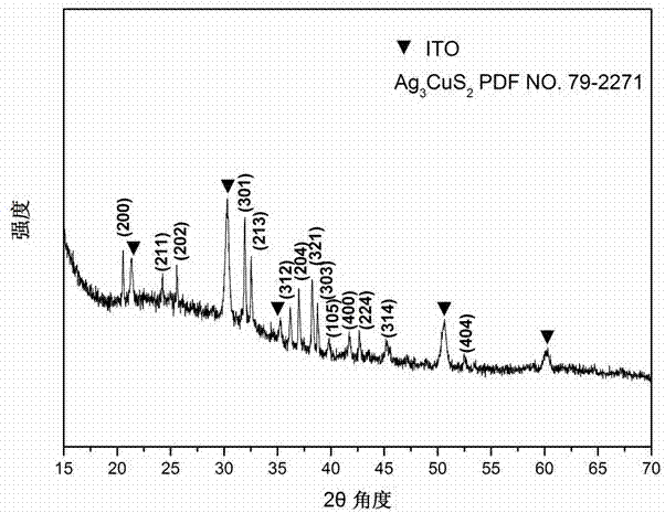
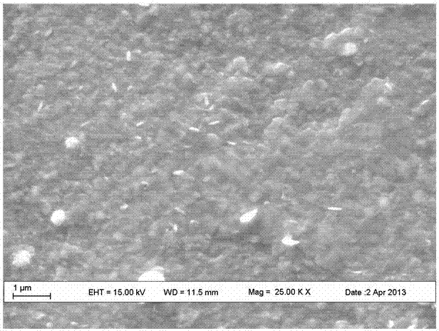
[0047] 3, aftertreatment: with embodiment 1, obtain Ag 3 CuS 2 Sulfur-copper-silver film samples. The color of the product is gray-black, and the microstructure under the scanning electron microscope is granular crystals. Scanning electron microscope photos see ( diagram 2-1 ), XRD results see ( Figure 2-2 ).

Embodiment 3

[0049] 1, preparatory work: with embodiment 1.

[0050] 2. Reaction steps: Weigh 0.05g of sulfur powder and put it in a petri dish with a diameter of 100mm, add absolute ethanol, the amount is subject to the sample that can be submerged in step 1, and prepare the copper-silver metal layer prepared in step 1 Place the ITO conductive glass flat in the petri dish, ensure that the sputtered metal layer is upward, avoid direct contact with the sulfur powder, place the petri dish in a stable place, and wait for 18 o Reaction under C conditions for 2.5 hours;

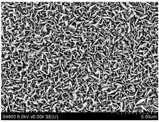
[0051] 3, aftertreatment: with embodiment 1, obtain Ag 3 CuS 2 Sulfur-copper-silver film samples. The color of the product is gray-black, and the microstructure under the scanning electron microscope is flaky nanocrystals. Scanning electron microscope photos see ( Figure 3-1 ), XRD results see ( Figure 3-2 ).


PUM


Abstract

The invention provides a chemical method for in-situ control and synthesis of an AgCuS / Ag3CuS2 ternary semiconductor photoelectric thin-film material at a normal temperature. According to the chemical method, a base material sputtered with elemental metal copper and elemental metal silver on the surface, or a copper-silver alloy foil material is placed into a container containing elemental sulfur powder and absolute ethyl alcohol obliquely, vertically or horizontally and prevented from being contacted with sulfur powder directly, and the base material is soaked under an organic solvent liquid level and react for 25 min to 12 h at a temperature ranging from 18 DEG C to 40 DEG C. During a reaction process, the concentration of the elemental sulfur powder is maintained in a saturation state; the ash black AgCuS / Ag3CuS2 ternary photoelectric thin-film semiconductor material is prepared in situ on the surface of the base materials after the reaction is finished; and a product is washed by absolute ethyl alcohol and dried at a room temperature. The method is low in energy consumption, the reaction vessel is simple, the used solvent can be reused, a surfactant and other chemical additives are not needed to use, post-processing of the product is simple, and the method has bright industrial application prospects.

Description

technical field [0001] The invention belongs to the technical field of material chemistry, and in particular relates to a chemical method for large-area in-situ controlled synthesis of sulfur-copper-silver ternary compound semiconductor photoelectric film materials at normal temperature. Background technique [0002] Sulfur-copper-silver ternary compound was discovered in 1858 Breithaupt Since its discovery, it has attracted widespread attention due to its many interesting physical properties, including: phase transition at different temperatures, fast ion conductor, gas-sensing properties, etc. Sulfur-copper-silver thin film materials are also an important part of commercial copper ion selective electrodes. In the preparation process of sulfur-copper-silver ternary compound materials, the two elements of copper and silver can be controlled, and compounds with different atomic ratios can be prepared, so as to further control their forbidden band width and realize the ab...

Claims


Application Information

Patent Timeline
IPC IPC(8): H01L31/18H01L31/032C01G9/00
CPCY02P70/50
Inventor 郑直雷岩范丽波刘松子贾会敏程佳美
Owner XUCHANG UNIV
Learn More