Annular laser device with electrode group and manufacture method for electrode group
A technology of ring lasers and electrode groups, which is applied to lasers, laser parts, laser parts, etc., can solve the problems of long sealing period, cracking of resonant cavity, large thermal residual stress and deformation, etc., and achieve simple manufacturing method Reliability, easy disassembly or replacement, and enhanced maintainability
- Summary
- Abstract
- Description
- Claims
- Application Information
AI Technical Summary
Problems solved by technology
Method used
Image

Examples
Embodiment 1
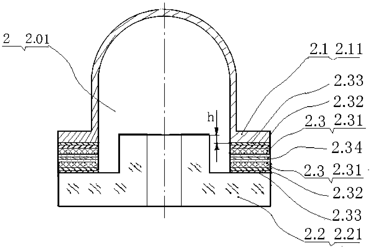
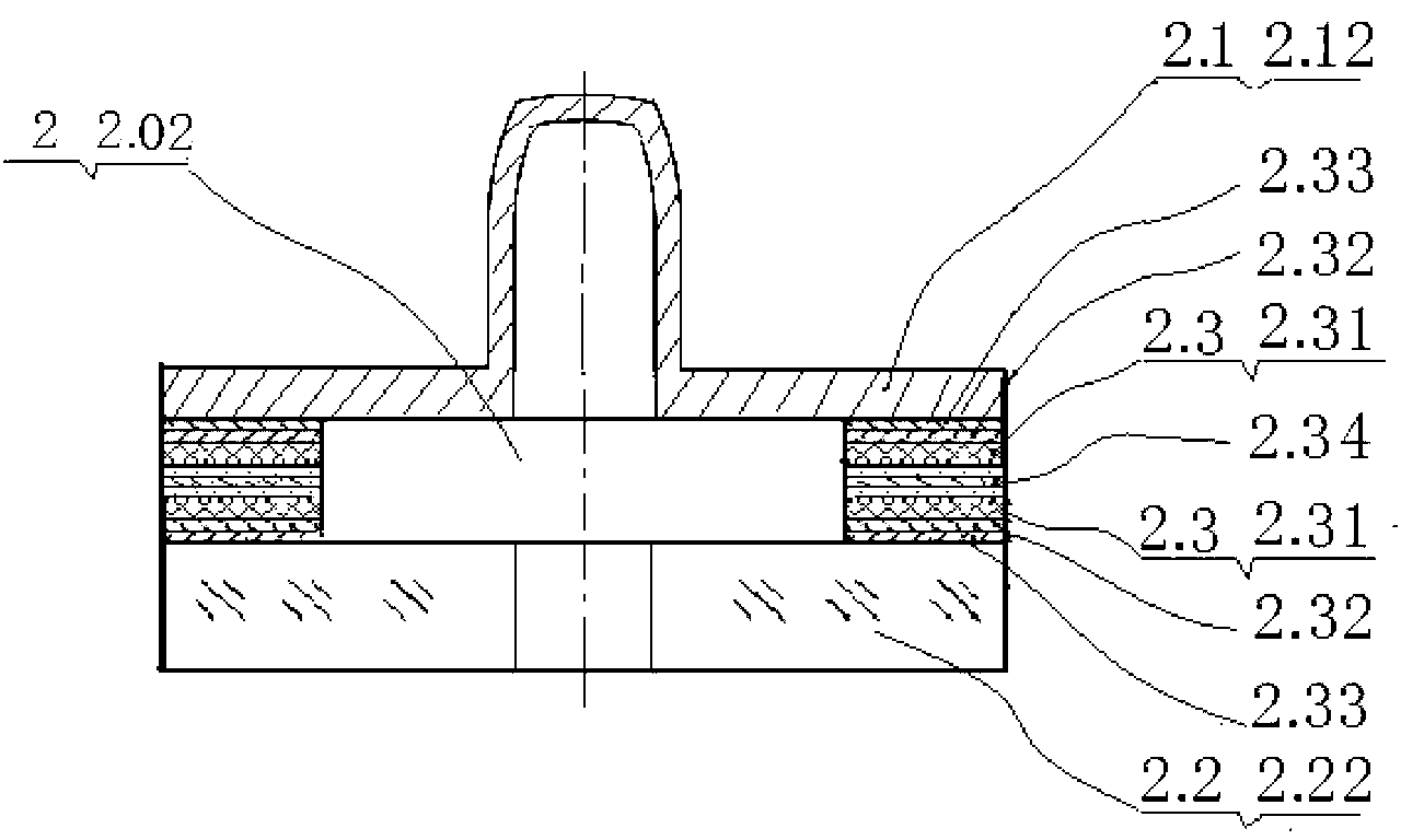
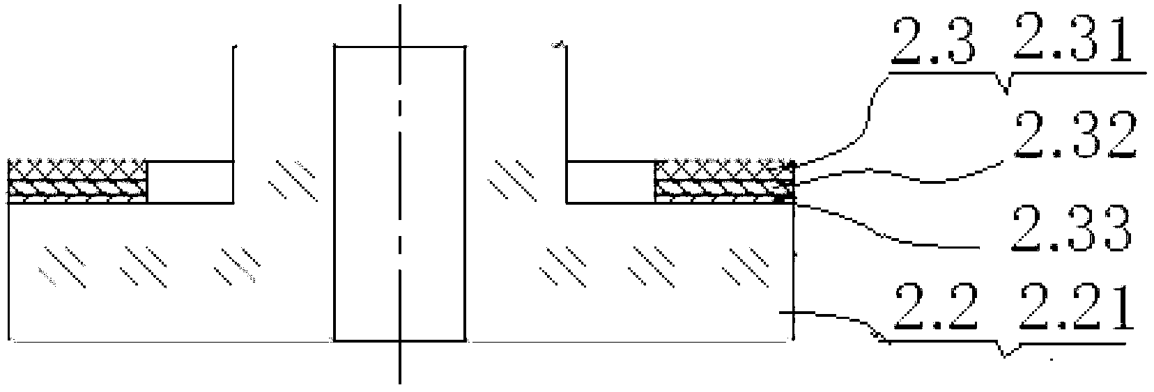
[0040] Example 1: It is a basic embodiment of a ring laser with an electrode group in the present invention, including a resonant cavity 1, which includes an electrode group 2, an optical mirror 3 and several light passages; the optical mirror 3 includes a light splitter Prism 3.1, light-combining prism 3.2, reflector 3.3, E-shaped mirror 3.4; there is also a detector 5 on the resonance cavity 1; the inside of the resonance cavity 1 is filled with helium-neon mixed gas; the electrode group 2 is composed of an electrode conductor 2.1 It is connected with the glass ring piece 2.2 through the connection layer 2.3 by thermocompression; the connection layer 2.3 is: the seed layer 2.33 deposited on the sealing position opposite to the electrode conductor 2.1 and the glass ring piece 2.2, and the seed layer 2.33 deposited on the The transition layer 2.32, the active reaction layer 2.31 made on the transition layer 2.32, and the solder layer ring sheet 2.34 sandwiched between the act...
Embodiment 2
[0041] Example 2: It is the preferred technical solution. The difference from the above-mentioned embodiment 1 is: the anode electrode group 2.02 has a small anode electrode group 2.02' and a large anode electrode group 2.02''. The material of the glass ring 2.2 is the same as that of the resonant cavity 1, mainly selected from glass-ceramics or silicon dioxide; the material of the electrode conductor 2.1 is a metal material.
Embodiment 3
[0042] Example 3: It is the preferred technical solution. The difference from the above-mentioned embodiment 1 is that the materials of the seed layer 2.33 and the transition layer 2.32 are both metal. The active reaction layer 2.31 is a layered structure made of two or more materials with mixed negative calorific values through alternate evaporation of nanometer thin films, or by screen printing of nanometer particles. The material of the seed layer 2.33 is mainly Cr, the material of the transition layer 2.32 is mainly Au, and the material of the active reaction layer 2.31 is selected from two or more combinations of Al, Ni, Ti, Si, Nb and Mo. The material of the solder layer ring piece 2.34 is high melting point solder selected from gold-tin alloy solder or tin-silver-copper alloy solder.
PUM
 Abstract
Description
Claims
Application Information
 - R&D
- Intellectual Property
- Life Sciences
- Materials
- Tech Scout
- Unparalleled Data Quality
- Higher Quality Content
- 60% Fewer Hallucinations
Browse by: Latest US Patents, China's latest patents, Technical Efficacy Thesaurus, Application Domain, Technology Topic, Popular Technical Reports.
© 2025 PatSnap. All rights reserved.Legal|Privacy policy|Modern Slavery Act Transparency Statement|Sitemap|About US| Contact US: help@patsnap.com