Electric field induction rheology forming method of paraboloid-like microlens array

An electric field-induced rheology and micro-lens array technology, applied in lenses, optics, instruments, etc., can solve the problems of large optical surface roughness, affecting adoption and promotion, etc., and achieve the effect of reducing processing costs and improving processing efficiency.

Active Publication Date: 2013-07-10
XI AN JIAOTONG UNIV
View PDF3 Cites 4 Cited by
  • Summary
  • Abstract
  • Description
  • Claims
  • Application Information

AI Technical Summary

Problems solved by technology

However, these methods can only prepare spherical microlenses, and the optical surface roughness obtained by the method of material removal or ablation is large, which seriously affects its adoption and promotion in the application field

Method used


Image

  • Electric field induction rheology forming method of paraboloid-like microlens array
  • Electric field induction rheology forming method of paraboloid-like microlens array
  • Electric field induction rheology forming method of paraboloid-like microlens array

Examples


Embodiment Construction

[0020] The present invention will be described in detail below in conjunction with the accompanying drawings.

[0021] An electric field-induced rheological deformation method of a parabolic microlens array, comprising the following steps:

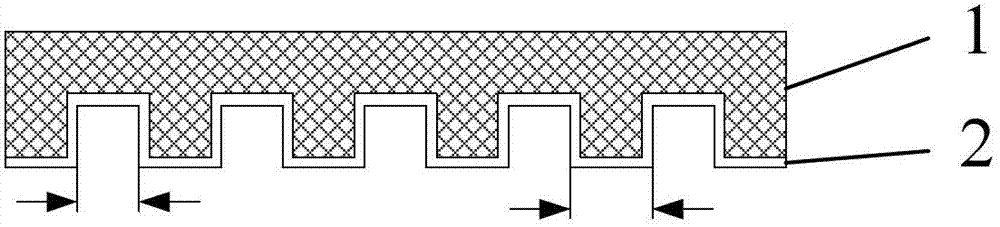
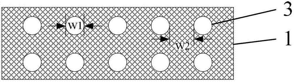
[0022] 1) Preparation and processing of the upper plate mold: Referring to Figure 1, the upper plate mold 1 adopts the traditional process of photolithography and etching to make the microhole array 3 on the wafer, and then thermally heats it on the surface of the patterned wafer. Oxidize the SiO2 dielectric layer 2 with a thickness of 1um. After completion, use the surface treatment agent F1060 to treat the surface of the wafer with low surface energy to prevent damage to the lens array structure during demoulding;

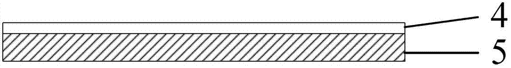
[0023] 2) Selection of lower plate and polymer: prepare transparent conductive ITO glass as the lower plate, and its preparation method is as follows: refer to figure 2 , using PECVD technology to vapor-deposit a layer of 5...


PUM


Abstract

Provided is an electric field induction rheology forming method of a paraboloid-like microlens array. A photoetching method is firstly used for preparing and processing an upper counter electrode hole mold, then a transparent electric-conduction indium tin oxide (ITO) glass lower counter electrode, after a direct current external electric field is exerted between the upper counter electrode and the lower counter electrode, polymer is dropped in an opening of a gap between the upper counter electrode and the lower counter electrode, the liquid level height and the shape of the polymer flowing into the gap between the upper counter electrode and the lower counter electrode are controlled by the electric field, curing and demoulding are carried out, and a paraboloid-like micro-concave-lens array is obtained; and then replication is carried out on the paraboloid-like micro-concave-lens array to finally obtain a paraboloid-like micro-convex-lens array. The method breaks through the limitation that a conventional microlens array preparation process can only be used for preparing a spherical lens, the obtained microlens array has a super-smooth surface and is better than a lens array obtained through material removal or a corrosion method, meanwhile, due to the fact that complex process control is not needed in the method, processing cost is greatly lowered, processing efficiency is improved, and the electric field induction rheology forming method can be widely used for a chip laboratory, a flat-panel display, optical system detection and observation and other respects.

Description

technical field [0001] The invention belongs to the technical field of micro-nano manufacturing, and in particular relates to an electric field-induced rheological deformation method of a parabolic micro-lens array. Background technique [0002] Microlens refers to tiny lenses, usually with a diameter of 10 μm to 1 mm, and according to the different surface curvatures, microlenses can be divided into spherical microlenses and aspheric microlenses, of which aspheric microlenses can better eliminate Spherical aberration is more practical, and the array composed of these tiny lenses according to a certain filling rate and arrangement is a microlens array. In view of its huge application in many fields such as communication technology, optical measurement, flat panel display and imaging, various preparation methods for microlens arrays have been proposed, such as photoresist hot-melt method, inkjet printing method and excimer laser ablation. law etc. However, these methods can...

Claims


Application Information

Patent Timeline
Patent Type & Authority Applications(China)
IPC IPC(8): G02B3/00
Inventor 丁玉成邵金友姜承宝李祥明田洪淼胡鸿
Owner XI AN JIAOTONG UNIV
Why Eureka
Try Eureka