Electric field induction imprinting method of aspheric surface micro-lens array

A technology of microlens array and electric field induction, which is applied in the direction of lens, photoplate making process of pattern surface, optics, etc., can solve the problems affecting the adoption and promotion, and achieve the effect of reducing processing cost and improving processing efficiency

Active Publication Date: 2015-07-08
XI AN JIAOTONG UNIV
View PDF5 Cites 0 Cited by
  • Summary
  • Abstract
  • Description
  • Claims
  • Application Information

AI Technical Summary

Problems solved by technology

However, these methods can only prepare spherical microlenses, which seriously affects its adoption and promotion in the field of application.

Method used


Image

  • Electric field induction imprinting method of aspheric surface micro-lens array
  • Electric field induction imprinting method of aspheric surface micro-lens array
  • Electric field induction imprinting method of aspheric surface micro-lens array

Examples


Embodiment Construction

[0023] The present invention will be described in detail below in conjunction with the accompanying drawings.

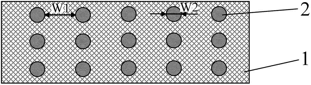
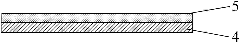
[0024] Press the imprinting mold with a pressure of 10Mpa on the surface of the conductive substrate coated with the polymer in advance, so that the imprinting mold and the substrate are tightly combined, and ensure that the ambient temperature is above the glass transition temperature of the polymer, so as to realize the polymer in the press. Complete filling in the cavity of the stamping mold, and then cooling to room temperature for demoulding to obtain a polymer microcolumn array on a conductive substrate. Use another conductive electrode plate as the upper electrode to form a pair of parallel electrode pairs with the substrate. A DC voltage of 300-500V is applied, and the ambient temperature is raised above the glass transition temperature of the polymer. Under the induction of the electric field force, the polymer micropillar array re-rheologically shapes, and a...


PUM

PropertyMeasurementUnit
thicknessaaaaaaaaaa

Abstract

Disclosed is an electric field induction imprinting method of an aspheric surface micro-lens array. A micro-column array is placed on information technology outsourcing (ITO) conducting glass base materials in an imprinting mode, then another piece of ITO conducting glass is used as a top electrode, then a pair of parallel plate electrodes are formed with the base materials, and direct voltage is applied between the electrodes. When the base materials are heated to a temperature higher than a glassy state transition temperature of a polymer, under the induction impact of an electric field, the micro-column array deforms into the aspheric surface micro-lens array in a flowing mode, and the specific steps includes preparing and processing a imprinting mould, then selecting the base materials, electrodes and the polymer, then imprinting, demolding, applying an external electric field to conduct electric field induction remolding, and last, the polymer is solidified and the aspheric surface micro-lens array is acquired. The electric field induction imprinting method of the aspheric surface micro-lens array does not need complex process control, greatly reduces processing cost and improves processing efficiency.

Description

technical field [0001] The invention belongs to the technical field of micro-nano manufacturing, and in particular relates to an electric field-induced embossing method for an aspheric micro-lens array. Background technique [0002] Microlens refers to tiny lenses, usually with a diameter of 10 μm to 1 mm, and according to the different surface curvatures, microlenses can be divided into spherical microlenses and aspheric microlenses, of which aspheric microlenses can better eliminate Spherical aberration is more practical, and the array composed of these tiny lenses according to a certain filling rate and arrangement is a microlens array. In view of its huge application in many fields such as communication technology, optical measurement, flat panel display and imaging, various preparation methods for microlens arrays have been proposed, such as photoresist hot-melt method, inkjet printing method and excimer laser ablation. law etc. However, these methods can only prepare...

Claims


Application Information

Patent Timeline
Patent Type & Authority Patents(China)
IPC IPC(8): G02B3/02G03F7/00
Inventor 邵金友丁玉成胡鸿田洪淼李祥明
Owner XI AN JIAOTONG UNIV
Why Eureka
Try Eureka