Mask plate, manufacturing method thereof, and exposure method of photoresist layer

A production method and a technology of a photoresist layer are applied in the field of semiconductors to achieve the effect of avoiding diffraction phenomenon, good monochromaticity and directivity

Active Publication Date: 2015-09-02
SEMICON MFG INT (SHANGHAI) CORP
View PDF5 Cites 0 Cited by
  • Summary
  • Abstract
  • Description
  • Claims
  • Application Information

AI Technical Summary

Problems solved by technology

However, due to the existence of diffraction phenomenon when the light passes through the mask, the above technologies for improving the resolution of lithography will encounter the limit when the feature size of the pattern becomes smaller and smaller.
[0007] In the prior art, there are many patent documents about mask plates, such as the “method of repairing a polymer mask” disclosed by US Patent Application Publication No. US2009 / 0095922A1 published on April 16, 2009. method)", however, none of the above technical problems have been solved

Method used


Image

  • Mask plate, manufacturing method thereof, and exposure method of photoresist layer
  • Mask plate, manufacturing method thereof, and exposure method of photoresist layer
  • Mask plate, manufacturing method thereof, and exposure method of photoresist layer

Examples


Embodiment Construction

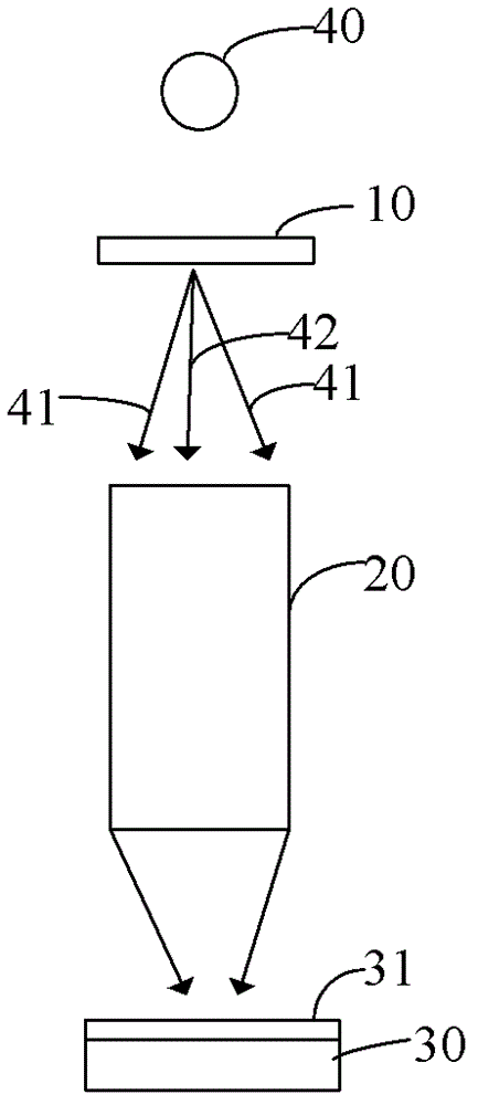
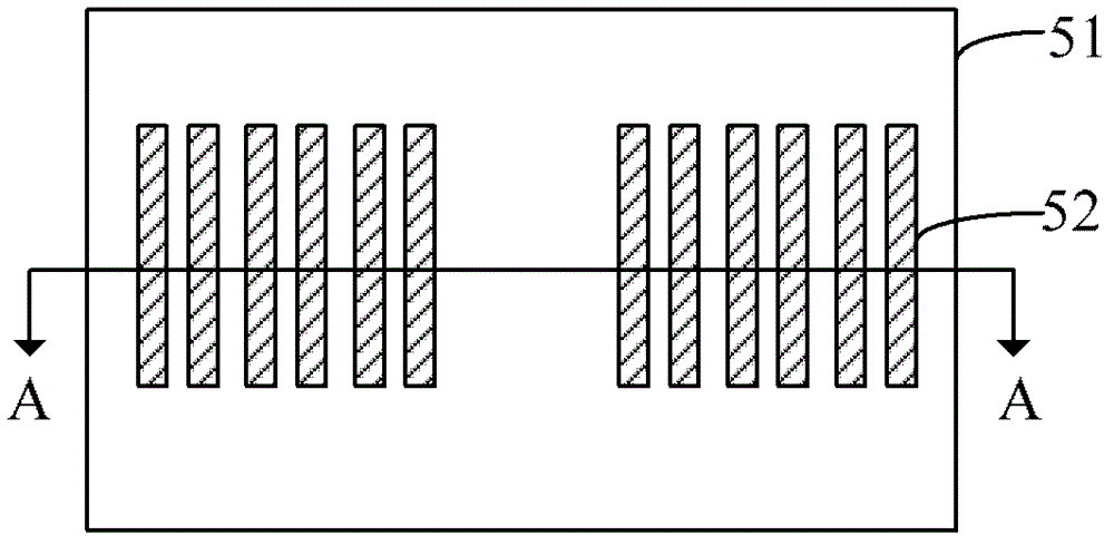
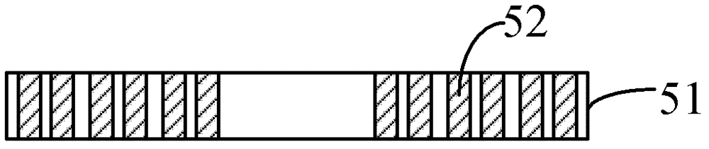
[0035] In order to make the above objects, features and advantages of the present invention more comprehensible, specific implementations of the present invention will be described in detail below in conjunction with the accompanying drawings.

[0036] In the following description, specific details are set forth in order to provide a thorough understanding of the present invention. However, the present invention can be implemented in many other ways than those described here, and those skilled in the art can make similar extensions without departing from the connotation of the present invention. Accordingly, the present invention is not limited to the specific embodiments disclosed below.

[0037] The inventor found through research that electrons can jump from one energy level to another energy level by absorbing or releasing energy. When an electron absorbs a photon, it may jump from a lower energy level to a higher energy level. Likewise, an electron at a higher energy le...


PUM


Abstract

The invention relates to a mask, a manufacturing method of the mask and a method for exposing a photoresist layer. The mask comprises a transparent substrate; a reserved region of the transparent substrate is provided with doping ions; a graph on the mask is formed by the reserved region with the doping ions; the doping ions implement transition from low energy level to high energy level under the irradiation of pump light; after implementing the transition from low energy level to high energy level, the doping ions generate transmitted light under the irradiation of induction light; the wavelength, phase, amplitude and propagation direction of the transmitted light are all the same with those of the induction light; and the light intensity of the transmitted light is higher than those of the induction light and the pump light. The technical scheme changes a conventional method for exposing the photoresist layer, so that the phenomenon of diffraction generated when light passes through the mask is avoided and no matter what extent the feature size of the graph is reduced to, the mask can be utilized to carry out a process for exposing the photoresist layer.

Description

technical field [0001] The invention relates to the technical field of semiconductors, in particular to a mask plate, a manufacturing method thereof, and an exposure method of a photoresist layer. Background technique [0002] In the semiconductor manufacturing process, the photolithography process plays a central role and is the most important process step in the production of integrated circuits. With the development of semiconductor manufacturing technology, the feature size is getting smaller and smaller, and the requirements for resolution in the photolithography process are getting higher and higher. Lithography resolution refers to the minimum feature size that can be exposed on the surface of a silicon wafer by a lithography machine, and is one of the important performance indicators in lithography technology. [0003] figure 1 It is a schematic diagram in the prior art where light is irradiated onto a silicon wafer with a photoresist layer after passing through a ...

Claims


Application Information

Patent Timeline
Patent Type & Authority Patents(China)
IPC IPC(8): G03F1/50G03F7/20
Inventor 王辉顾一鸣
Owner SEMICON MFG INT (SHANGHAI) CORP
Why Eureka
Try Eureka