On-chip clock generating circuit with lower power consumption
A clock generation circuit and generation circuit technology are applied in the field of low-power on-chip clock generation circuit and ADC sampling clock circuit, which can solve the problems of large deviation of clock frequency, power supply voltage and temperature variation, achieve small chip area and improve stability. and the effect of integration
- Summary
- Abstract
- Description
- Claims
- Application Information
AI Technical Summary
Problems solved by technology
Method used
Image
Examples
no. 2 example
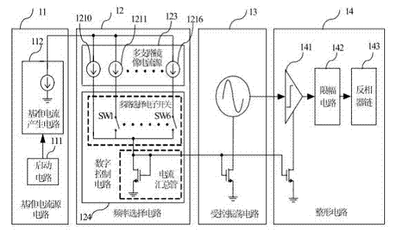
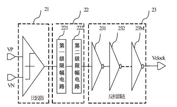
[0056] figure 2A structural block diagram of the shaping circuit 14 of the embodiment of the present invention is given, which is composed of a comparator 21 , a limiter circuit 22 and an inverter chain 23 . Limiter circuit 22 is made up of cascaded first limiter circuit 221 and second limiter circuit 222, and inverter chain 23 is made up of M cascaded inverters, and M inverters are respectively 231, 232, ..., 23N. VP and VN are the differential input signal terminals of the shaping circuit, receiving the differential oscillation output of the control oscillation circuit 13; Vclock is the output terminal of the shaping circuit, and also the clock signal output of the entire low-power on-chip clock generation circuit, and the output clock signal is used for As a reference clock signal for other circuits.
no. 3 example
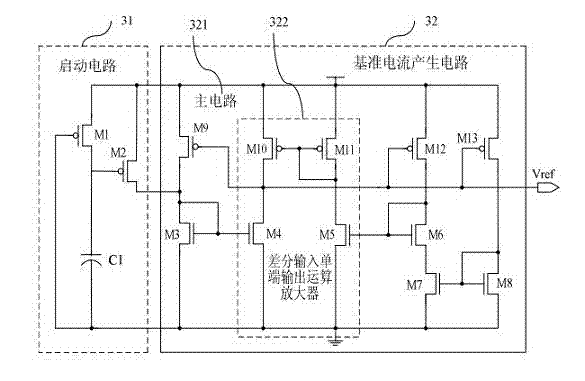
[0058] image 3 The circuit composition diagram of the reference current source circuit of the embodiment of the present invention is given; the reference current source circuit 11 is composed of a starting circuit 31 and a reference current generating circuit 32 . The startup circuit 31 is composed of a capacitor C1 and two PMOS transistors M1 and M2. The startup circuit 31 is connected to a reference current generation circuit 32 . When power on, when the power supply voltage rises from zero, when the power supply voltage rises to a certain value, the M1 and M2 tubes are turned on, and at this time, the M2 tube injects a certain current into the main circuit of the reference current generating circuit 32 to make the reference current The generating circuit 32 gets rid of the degeneracy bias point and enters a normal working state, and at the same time, the M1 tube charges the capacitor C1. With the charging of the capacitor, when the voltage value on C1 increases to make t...
no. 4 example
[0061] Figure 4 The circuit composition diagram of the frequency selection circuit of the embodiment of the present invention where N is 7 is given, which consists of 8 mirror current sources 41 with N being 7 and a digital control circuit 42 with 7 electronic switches and current summarization circuits. The PMOS tubes M0-M7 form an 8-branch mirror current source with N being 7, and their currents are all mirrored to the reference mirror current output by the reference current generating circuit 32. The channel lengths of the tubes M0-M7 are the same, and the channel lengths of the tubes M0 and M1 are the same. The widths are the same, the widths of the tubes M1-M7 are multiplied exponentially, and the ratio of the widths of the tubes M0-M7 is 1:1:2:4:8:16:32:64. The tubes M8-M14 form a 7-bit configurable PMOS switch tube array, and V1-V7 are 7 digital control words, which respectively control the on or off of the switches of the seven PMOS tubes M8-M14. Among them, the fixe...
PUM
 Abstract
Description
Claims
Application Information
 - Generate Ideas
- Intellectual Property
- Life Sciences
- Materials
- Tech Scout
- Unparalleled Data Quality
- Higher Quality Content
- 60% Fewer Hallucinations
Browse by: Latest US Patents, China's latest patents, Technical Efficacy Thesaurus, Application Domain, Technology Topic, Popular Technical Reports.
© 2025 PatSnap. All rights reserved.Legal|Privacy policy|Modern Slavery Act Transparency Statement|Sitemap|About US| Contact US: help@patsnap.com


