N-type implanted infrared-to-visible wavelength up-conversion device and preparation method thereof
A conversion device, N-type technology, applied in the direction of sustainable manufacturing/processing, climate sustainability, final product manufacturing, etc., can solve the problems of difficult injection of photogenerated holes, low conversion efficiency, low light utilization efficiency, etc., to promote The effect of high transmission and conversion efficiency and improved detection rate
- Summary
- Abstract
- Description
- Claims
- Application Information
AI Technical Summary
Problems solved by technology
Method used
Image
Examples
preparation example Construction
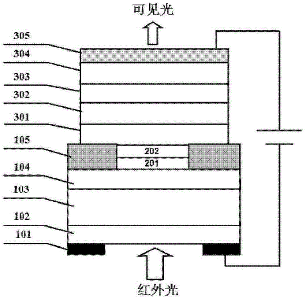
[0043] Figure 4 A flow chart of the preparation method of the N-type implanted infrared-to-visible wavelength up-conversion device proposed by the present invention is shown. Such as Figure 4 As shown, the present invention also proposes a specific preparation method of an N-type implanted infrared-to-visible wavelength up-conversion device, which includes the following steps:
[0044] Step 1, using semiconductor thin film epitaxy techniques such as molecular beam epitaxy (MBE) or metal organic chemical vapor deposition (MOCVD) to grow the material structure of the infrared detector unit 103 on the substrate 102; then grow N-type on the infrared detector unit 103 spacer layer 104 .
[0045] Step 2, using semiconductor processing technology to prepare the device structure of the infrared detector unit 103;
[0046] Step 3, making the cathode layer 101 on the back side of the substrate 102;
[0047] Step 4, preparing an insulating window layer 105 on the top of the N-type ...
Embodiment 1
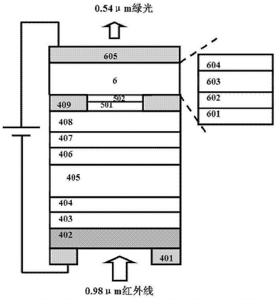
[0057] figure 2 It shows a schematic cross-sectional view of the N-type implanted infrared-to-visible wavelength up-conversion device in a preferred embodiment of the present invention, wherein the inorganic infrared detector unit is based on a GaAs / InGaAs multiple quantum well structure. The N-type implanted infrared-to-visible wavelength up-conversion imaging device can realize up-conversion of wavelengths from 0.98 μm to 0.54 μm, and its preparation method is as follows:
[0058] Step 1. Using a molecular beam epitaxy system to epitaxially grow an infrared detector unit on a P-type GaAs substrate 402, the details are as follows:
[0059] 1) Epitaxially grow a P-type GaAs buffer layer 403 on a P-type GaAs substrate 402 with a thickness of 200 nm and a P-type doping concentration of 3×10 18 cm -3 ;
[0060] 2) epitaxially growing an intrinsic GaAs layer 404 on the P-type GaAs buffer layer 403 with a thickness of 5 nm;
[0061] 3) Epitaxial growth of 60 cycles of GaAs / In ...
PUM
 Abstract
Description
Claims
Application Information
 - R&D
- Intellectual Property
- Life Sciences
- Materials
- Tech Scout
- Unparalleled Data Quality
- Higher Quality Content
- 60% Fewer Hallucinations
Browse by: Latest US Patents, China's latest patents, Technical Efficacy Thesaurus, Application Domain, Technology Topic, Popular Technical Reports.
© 2025 PatSnap. All rights reserved.Legal|Privacy policy|Modern Slavery Act Transparency Statement|Sitemap|About US| Contact US: help@patsnap.com


