Back process method of IGBT (insulated gate bipolar transistor) device

A backside process and device technology, which is applied in semiconductor/solid-state device manufacturing, electrical components, circuits, etc., can solve the problems of shallow junction, no obvious improvement, and low activation rate of the surface layer, and achieve high activation efficiency.

Active Publication Date: 2013-04-17
SHANGHAI HUAHONG GRACE SEMICON MFG CORP
View PDF2 Cites 11 Cited by
  • Summary
  • Abstract
  • Description
  • Claims
  • Application Information

AI Technical Summary

Problems solved by technology

It can be seen that when the laser energy is low, the activation rate of the surface layer is not high and the junction depth is shallow. When the energy is high, diffusion will occur, but the peak concentration on the surface will decrease, and the total activation rate is equivalent to that of lower energy. Significantly improved

Method used


Image

  • Back process method of IGBT (insulated gate bipolar transistor) device
  • Back process method of IGBT (insulated gate bipolar transistor) device
  • Back process method of IGBT (insulated gate bipolar transistor) device

Examples


Embodiment Construction

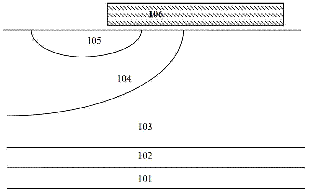
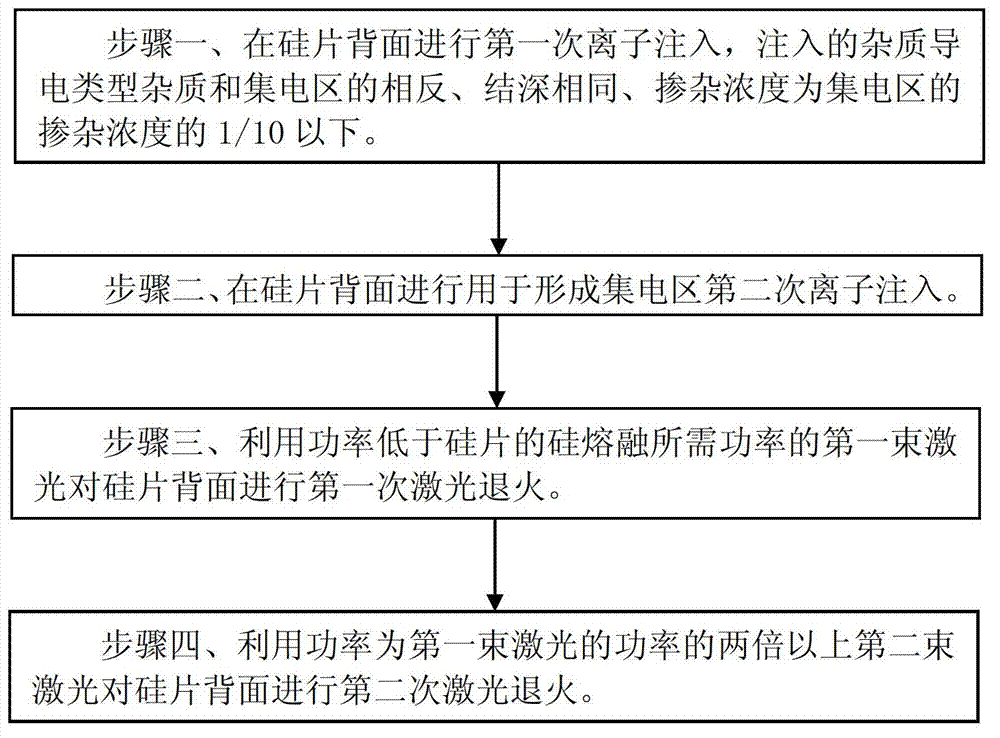
[0033] Such as figure 2 As shown, it is a flow chart of the method of the embodiment of the present invention; the backside process method of the IGBT device of the embodiment of the present invention adopts the following steps to form the collector region with P-type doping of the IGBT device:

[0034] Step 1. Perform the first ion implantation on the back of the silicon wafer. The impurities of the first ion implantation are N-type impurities. The implantation depth of the first ion implantation and the subsequent formation of the second ion implantation of the collector region The implantation depths are the same, and the doping concentration of the N-type impurity in the first ion implantation is less than 1 / 10 of the doping concentration of the P-type impurity in the collector region. The implantation energy of the first ion implantation is 1kev-50kev, and the implantation dose is 1e12 atoms / cm 2 ~1e14 atoms / cm 2 1. The impurity implanted is phosphorus or arsenic, and ...


PUM


Abstract

The invention discloses a back process method of an IGBT (insulated gate bipolar transistor) device. A collector region of the IGBT device is formed by the following steps: the first time of ion implantation is carried out on the back of a silicon slice, impurities in the implantation are conduction type impurities which are opposite to those of the collector region, the junction depths are identical, and the dosage concentration of the impurities is less than 1/10 of the dosage concentration of the impurities in the collector region; the second time of ion implantation used for forming the collector region is carried out on the back of the silicon slice; the first time of laser annealing is carried out on the back of the silicon slice by a first bundle of laser of which the power is lower than the power needed for silicon fusing of the silicon slice; and the second time of laser annealing is carried out on the back of the silicon slice by a second bundle of laser of which the power is more than double the power of the first bundle of laser. According to the method disclosed by the invention, the collector region with a highly activated surface layer and a certain junction depth is formed by a laser annealing process, the demand of the device can be met, and the front process of the device can not be affected.

Description

technical field [0001] The invention relates to a semiconductor integrated circuit manufacturing process method, in particular to a back process method of an insulated gate bipolar transistor (Insulated gate bipolar transistor, IGBT) device. Background technique [0002] IGBT has both the voltage control of the insulated gate field effect transistor (MOSFET) and the low on-resistance and high withstand voltage characteristics of the bipolar transistor (BJT). It has voltage control, large input impedance, low drive power, and small on-resistance , Low switching loss and many other excellent characteristics, are widely used in medium and high power power electronic systems. [0003] The IGBT is a backside lead-out device such as figure 1 Shown is a schematic structural diagram of an existing field stop (Field Stop, FS) IGBT; it includes: a collector region 101 formed on the back of the silicon wafer consisting of a P+ region, and a collector region 101 formed above the collec...

Claims


Application Information

Patent Timeline
Patent Type & Authority Applications(China)
IPC IPC(8): H01L21/331H01L21/265
Inventor 王雷童宇峰刘尧
Owner SHANGHAI HUAHONG GRACE SEMICON MFG CORP
Why Eureka
Try Eureka