Printed circuit board and formation method thereof

A printed circuit board and circuit technology, applied in the directions of printed circuits, printed circuit manufacturing, printed circuit components, etc., can solve the problems of complex milling methods, increase process costs, and complex process flows, and achieve reduction in process costs and avoidance. Corrosion damage, the effect of improving process efficiency

Active Publication Date: 2013-04-10
JIANGNAN INST OF COMPUTING TECH
View PDF5 Cites 5 Cited by
  • Summary
  • Abstract
  • Description
  • Claims
  • Application Information

AI Technical Summary

Problems solved by technology

Especially for leads of different lengths, the method of milling is more complicated
2) The leads are removed by exposure, development, and etching, but this method increases the process cost, and the process flow is complicated and the efficiency is low
However, the process of forming the lead wire and removing the lead wire is relatively complicated, which increases the process cost, and the process flow is complicated and the efficiency is low

Method used


Image

  • Printed circuit board and formation method thereof
  • Printed circuit board and formation method thereof
  • Printed circuit board and formation method thereof

Examples


Embodiment Construction

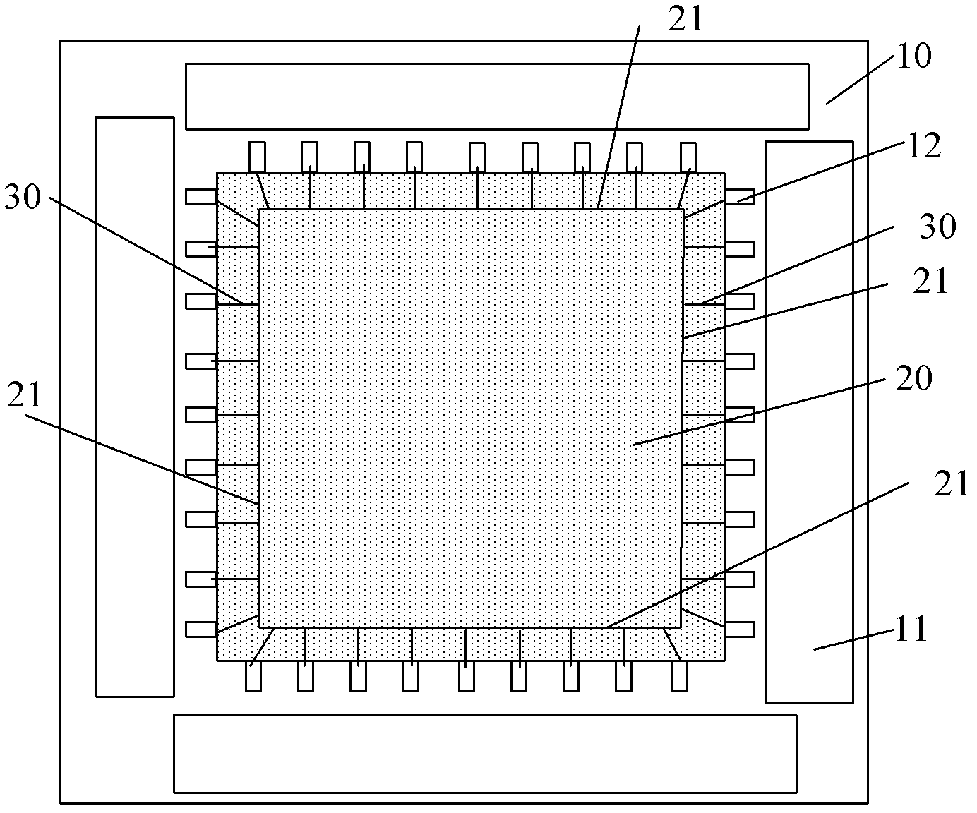
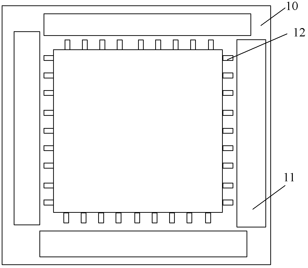
[0044] In the prior art, when performing an electroplating process on a printed circuit board, it is necessary to electrically connect the circuit to an external power source through a lead wire, so that the current is transmitted from the external power source to the circuit to achieve the purpose of electroplating metal. However, the processes of forming the lead wires and removing the lead wires are relatively complicated, which increases the process cost, and the process flow is complicated and the efficiency is low.

[0045] In order to solve the above problems, the present invention provides a printed circuit board, comprising:

[0046] a substrate, on which a first region and a second region are formed, and the first region is arranged around the second region;

[0047] Lines are arranged in the first area, and a conductive area is formed in the second area;

[0048] Wherein, all the lines in the first area are connected to the conductive area, and are in a state of fu...


PUM


Abstract

A printed circuit board comprises a substrate, wherein a first area and a second area are formed on the substrate, and the first area is arranged around the second area. A line is distributed at the first area, and a conductive area is formed at the second area. The line of the first area is electrically connected with the conductive area of the second area through wires, and the invention further provides a formation method of the printed circuit board. The line of the first area is electrically connected with the conductive area of the second area through the wires, and the second area is eliminated through adoption of a physical method so as to eliminate a short circuit. A method for eliminating the short circuit with the existing chemical process is replaced, and complexity of wire formation and wire elimination in the electroplating process is reduced. The electroplating process is simplified, process cost is reduced, technological process is simple, reliability of short circuit elimination is good, and efficiency is high.

Description

technical field [0001] The invention relates to the field of semiconductor packaging, in particular to a printed circuit board and a forming method thereof. Background technique [0002] With the continuous development of electronic products in the direction of multi-function, miniaturization, light weight, and high performance, the requirements for miniaturization and high density of printed circuit boards are also increasing. Wherein, the printed circuit board includes a substrate, a dielectric layer on the substrate and a conductive layer covering the surface of the dielectric layer. The conductive layer is a pre-designed circuit so that the chip is electrically connected to the printed circuit board. [0003] Forming circuits on the dielectric layer is an important step in the manufacturing process of printed circuit boards, including: providing a substrate on which a conductive layer is formed; laminating a dry film on the substrate; Expose the film; develop the expose...

Claims


Application Information

Patent Timeline
Patent Type & Authority Applications(China)
IPC IPC(8): H05K1/02H05K1/11H05K3/00H01L23/498H01L21/48
CPCH01L2224/49171
Inventor 徐杰栋刘晓阳刘秋华吴梅珠吴小龙梁少文郭永刚
Owner JIANGNAN INST OF COMPUTING TECH
Why Eureka
Try Eureka