
Improved method of bipolar integrated circuit amplification coefficient process

An integrated circuit and process improvement technology, applied in the field of semiconductor manufacturing process, can solve the problems of incomplete matching of stress characteristic circuits, attenuation of the amplification factor of bipolar circuits, etc., and achieve the effects of preventing attenuation, stabilizing the amplification factor of PNP tubes, and being easy to achieve.

Active Publication Date: 2013-04-03
EAST CHINA INST OF OPTOELECTRONICS INTEGRATEDDEVICE
View PDF3 Cites 3 Cited by
  • Summary
  • Abstract
  • Description
  • Claims
  • Application Information

AI Technical Summary

Problems solved by technology

[0003] The purpose of the present invention is to provide a bipolar integrated circuit amplification factor process improvement method to overcome the defect that the amplification factor of this type of bipolar circuit is attenuated due to the incomplete matching of the stress characteristics of the silicon nitride dielectric film and the circuit.

Method used


Image

  • Improved method of bipolar integrated circuit amplification coefficient process
  • Improved method of bipolar integrated circuit amplification coefficient process
  • Improved method of bipolar integrated circuit amplification coefficient process

Examples


Embodiment Construction

[0023] The method for improving the amplification factor process of a bipolar integrated circuit provided by the present invention includes the steps of manufacturing the basic circuit of a bipolar integrated circuit compatible with BJT and JFET by conventional technology, the step of manufacturing electrode leads on the basic circuit, and the subsequent process finishing step .

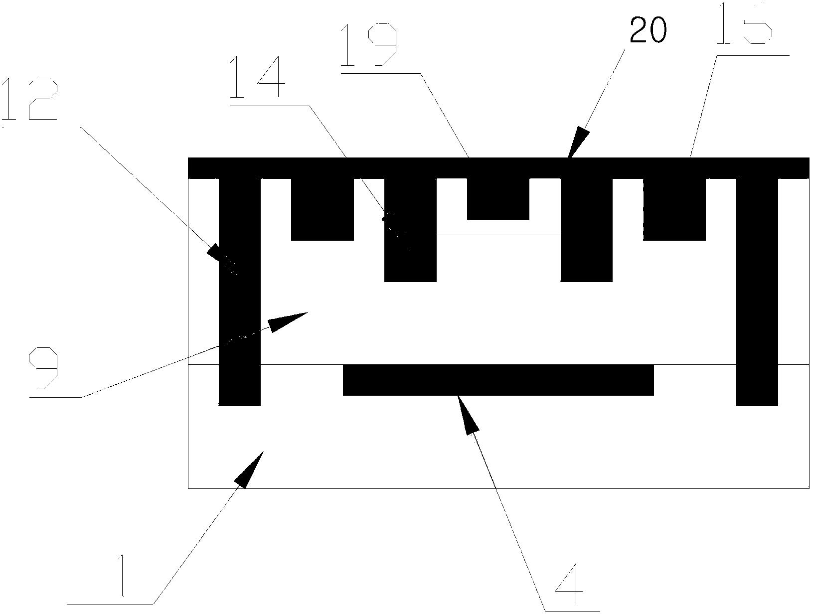
[0024] The basic circuit includes the underlying silicon P substrate 1, N - Epitaxial layer 9, P+ region 12, N+ region 4, base region boron (14), emitter region phosphorus (16) and gate region phosphorus (19).

[0025] The present invention is characterized in that the step of making electrode leads on the described basic circuit is:

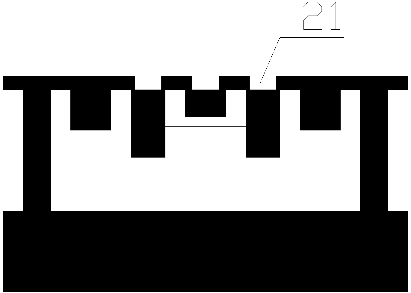
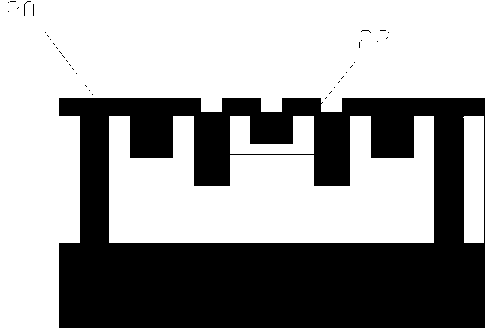
[0026] a. Depositing LTO - such as figure 1 As shown, at a furnace temperature of 420 ° C, a layer of silicon dioxide 20 of about 450 nm is deposited by LPCVD (vapor phase deposition device) as a circuit capacitor dielectric layer; then the deposited LTO layer is pro...


PUM


Abstract

The invention relates to an improved method of a bipolar integrated circuit amplification coefficient process, comprising a step of manufacturing a basic circuit of a bipolar integrated circuit compatible with a BJT (Bipolar Junction Transistor) and a JFET (Junction Field-Effect Transistor) by a conventional process, a step of manufacturing an electrode lead wire on the basic circuit and a step of carrying out follow-up process arrangement. The improved method is characterized in that the step of manufacturing the electrode lead wire on the basic circuit comprises the steps of: 1, primary photoetching and corrosion on a contact hole; 2, hole oxidization; 3, silicon nitride deposition; 4, secondary photoetching and hole secondary corrosion on the contact hole; 5, pure aluminum sputtering; and 6, formation of the electrode lead wire (25) and a press welding point by the photoetching and the corrosion. The improved method disclosed by the invention has the following advantages that (1) the stress of a silicon nitride dielectric film is effectively released so as to be matched with the property of bipolar circuits; (2) the attenuation of a PNP pipe amplification coefficient is effectively prevented and the PNP pipe amplification coefficient is stabilized; and (3) a technological approach is easy to realize.

Description

technical field [0001] The invention relates to the field of semiconductor manufacturing technology, in particular to a technology method for improving the amplification factor of a bipolar integrated circuit. Background technique [0002] The amplification factor is an important performance parameter index in the manufacture of bipolar integrated circuits, and its stability directly determines the reliability of the circuit. In some existing bipolar integrated circuit manufacturing processes compatible with BJT and JFET with silicon nitride, a silicon nitride dielectric film is used before the lead hole photolithography plate. Due to the stress characteristics of the silicon nitride dielectric film and the This kind of circuit is not completely matched. When testing the horizontal and vertical PNP tube amplification factors of this type of bipolar circuit, it shows that the contact hole is not connected or the ohmic contact between the aluminum lead and the silicon substrat...

Claims


Application Information

Patent Timeline
Patent Type & Authority Applications(China)
IPC IPC(8): H01L21/3213
Inventor 简崇玺陈计学吕东锋丁继洪张学明高博
Owner EAST CHINA INST OF OPTOELECTRONICS INTEGRATEDDEVICE
Learn More