How to make a bipolar transistor

A technology of bipolar transistors and manufacturing methods, which is applied in the direction of transistors, semiconductor/solid-state device manufacturing, semiconductor devices, etc., can solve problems affecting device reliability, damage, and unstable device amplification factors, and achieve high reliability and high amplification factors. stable effect

Inactive Publication Date: 2020-08-28
NANJING LISHUI HIGH-TECH VENTURE CAPITAL MANAGEMENT CO LTD
View PDF4 Cites 0 Cited by
  • Summary
  • Abstract
  • Description
  • Claims
  • Application Information

AI Technical Summary

Problems solved by technology

[0008] However, the most critical problem in the above-mentioned isolation sidewall manufacturing process is that the selection ratio of silicon nitride is not high enough during TEOS etching. Generally, about 15% over-etching is required to ensure that TEOS is etched clean. Over-etching is enough to etch away the underlying silicon nitride, which will inevitably damage the subsequent emitter surface, and the amplification factor (β) of the device will be extremely unstable, affecting the reliability of the device

Method used


Image

  • How to make a bipolar transistor
  • How to make a bipolar transistor
  • How to make a bipolar transistor

Examples


Embodiment Construction

[0034] The following will clearly and completely describe the technical solutions in the embodiments of the present invention. Obviously, the described embodiments are only some of the embodiments of the present invention, rather than all the embodiments. Based on the embodiments of the present invention, all other embodiments obtained by persons of ordinary skill in the art without making creative efforts belong to the protection scope of the present invention.

[0035] see Figure 1-Figure 13 , figure 1 It is a flow chart of the manufacturing method of the bipolar transistor of the present invention, Figure 2-Figure 13 for figure 1 The structural schematic diagram of each step of the manufacturing method of the bipolar transistor is shown. The manufacturing method of the bipolar transistor includes the following steps.

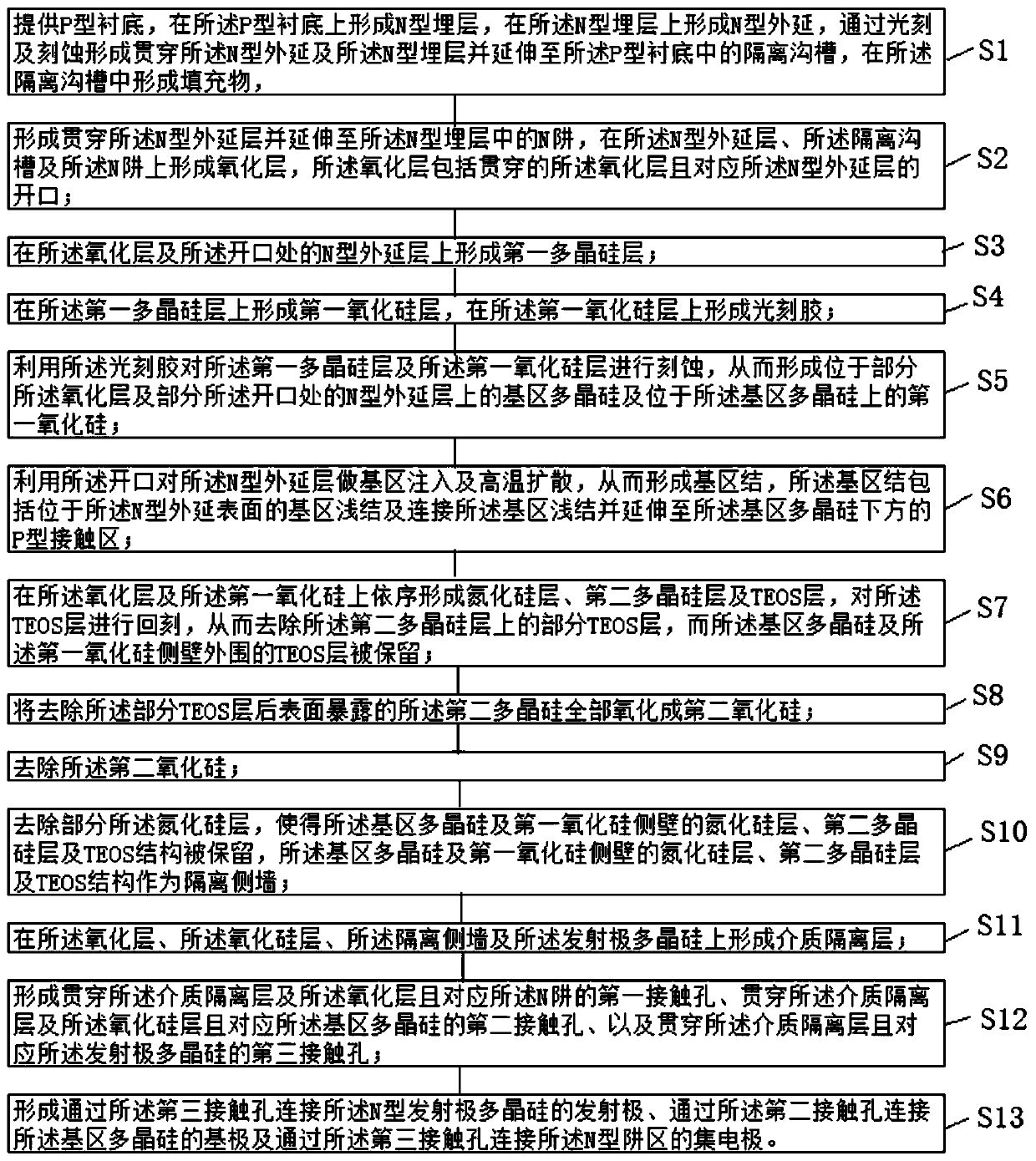
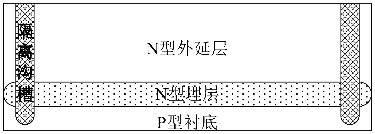
[0036] Step S1, see figure 2 , providing a P-type substrate, forming an N-type buried layer on the P-type substrate, forming an N-type epitaxial laye...


PUM

PropertyMeasurementUnit
thicknessaaaaaaaaaa
thicknessaaaaaaaaaa
thicknessaaaaaaaaaa

Abstract

The invention relates to a bipolar transistor manufacturing method. When isolation side walls between emitter electrode polysilicon and base electrode polysilicon are formed, the manufacturing methodcomprises following steps: sequentially forming a silicon nitride layer, a second polysilicon layer and a TEOS layer on an oxide layer and first silicon oxide, etching back the TEOS layer, thereby removing a part of the TEOS layer on the second polysilicon layer, and reserving the TEOS layer on the periphery of sidewalls of base region polysilicon and the first silicon oxide; oxidizing all the second polysilicon the surface of which is exposed after a part of the TEOS layer is removed to second silicon oxide; removing the second silicon oxide; removing a part of the silicon nitride layer, reserving the silicon nitride layer, the second polysilicon layer and the TEOS structure on the sidewalls of the base region polysilicon and the first silicon oxide, and taking the silicon nitride layer,the second polysilicon layer and the TEOS structure on the sidewalls of the base region olysilicon and the first silicon oxide as isolation side walls.

Description

【Technical field】 [0001] The invention relates to the technical field of semiconductor manufacturing technology, in particular, to a method for manufacturing a bipolar transistor. 【Background technique】 [0002] It originated from the point-contact transistor transistor invented in 1948, and developed into a junction transistor in the early 1950s, which is now called a bipolar transistor. There are two basic structures of bipolar transistors: PNP type and NPN type. In these three layers of semiconductors, the middle layer is called the base region, and the outer two layers are called the emitter region and the collector region. When a small amount of current is injected into the base region, a larger current will form between the emitter region and the collector region, which is the amplification effect of the transistor. In bipolar transistors, both electrons and holes conduct electricity. Compared with field effect transistors, bipolar transistors have slow switching sp...

Claims


Application Information

Patent Timeline
Patent Type & Authority Patents(China)
IPC IPC(8): H01L21/331H01L29/73
CPCH01L29/66234H01L29/73
Inventor 不公告发明人
Owner NANJING LISHUI HIGH-TECH VENTURE CAPITAL MANAGEMENT CO LTD
Why Eureka
Try Eureka