
Method for replacing helium atoms on film layer

A chlorine atom, film layer technology, used in the manufacture of discharge tubes, electrical components, semiconductor/solid state devices, etc.

Inactive Publication Date: 2013-03-06
SHENZHEN CHINA STAR OPTOELECTRONICS TECH CO LTD
View PDF2 Cites 4 Cited by
  • Summary
  • Abstract
  • Description
  • Claims
  • Application Information

AI Technical Summary

Problems solved by technology

In addition to improving the problem of re-etching in the prior art to avoid affecting the electrical properties of thin film transistors, the present invention also has the advantage of reducing the process time compared with the traditional process of using pure oxygen to improve the output.

Method used


Image

  • Method for replacing helium atoms on film layer

Examples


Embodiment Construction

[0024] In order to further set forth the technical means and effects that the present invention takes to achieve the purpose of the predetermined invention, below in conjunction with the accompanying drawings and preferred embodiments, its specific implementation, structure, Features and their functions are described in detail below.

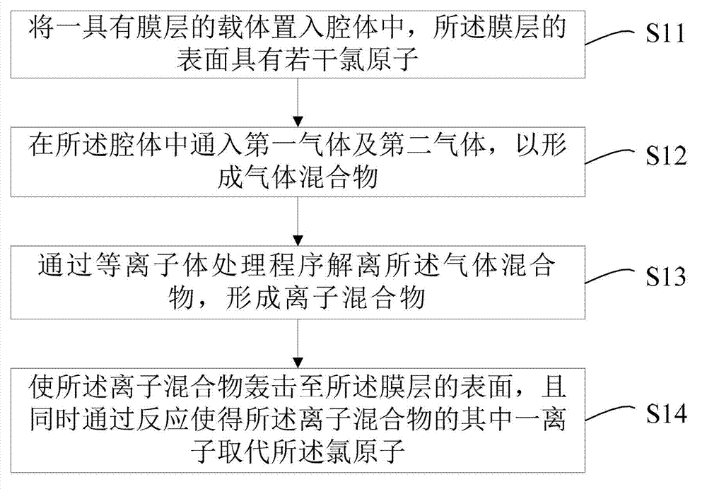
[0025] Please refer to figure 1 , which is a flow chart of the steps of the method for replacing chlorine atoms on the film layer in an embodiment of the present invention, the method includes the following steps S11-S14:

[0026] In step S11, a carrier with a film layer is placed into the cavity, and the surface of the film layer has several chlorine atoms. In this embodiment, step S11 is continued after the carrier with the film layer is etched by plasma as mentioned in the background art. Wherein, the film layer may be a metal layer, a semiconductor layer or an insulating layer.

[0027] In step S12, a first gas and a second gas are inject...


PUM


Abstract

The invention discloses a method for replacing helium atoms on a film layer. According to the method provided by the invention, the volume ratio of a gas inside gas mixture is reduced in a plasma treatment program (ions formed after that gas is dissociated can generate etching reaction with the film layer), so that replacing ions for replacing the helium atoms is sufficient after the gas mixture is dissociated. Therefore, the etching reaction on the film layer is reduced in a process of replacing the helium atoms. With the adoption of the method provided by the invention, the problem of re-etching in the prior art can be improved, so that the electricity of a thin film transistor can be prevented from being influenced. Compared with the conventional manufacturing process in which pure oxygen is used for treating, the method has the advantage of reducing the process time, so that the yield can be improved.

Description

technical field [0001] The present invention relates to a method for preventing corrosion and re-etching after etching, in particular to a method for replacing chlorine atoms on a film layer. Background technique [0002] The etching process (Etch process) can be divided into wet etching (Wet etching) and dry etching (Dry etching) two types. In wet etching, chemical solution is used to achieve the purpose of etching through chemical reaction, while dry etching is usually a kind of plasma etching (Plasma etching), and the etching mechanism of plasma etching is basically A physical interaction, the biggest advantage of which is Anisotropic etching. Anisotropic etching means that the etching action will only etch perpendicular to the active surface during the etching process, without causing undercut (Undercut) phenomenon, so it is suitable for high aspect ratio (Aspect Ratio) and grooves Etching requirements for components with a Cavity Width less than 2-3 μm (microns). [...

Claims


Application Information

Patent Timeline
IPC IPC(8): H01J37/32H01L21/02
CPCH01L21/32138H01L21/3065H01L21/3105
Inventor 郑扬霖
Owner SHENZHEN CHINA STAR OPTOELECTRONICS TECH CO LTD
Learn More