Integrated-type LED (light-emitting diode) light source heat radiating device and preparation method thereof
A technology of LED light source and heat dissipation device, which is applied in the field of integrated LED light source heat dissipation device and its preparation, and can solve the problems that it is difficult to meet the LED standard and device standard, the LED cannot reach a large power value, and the brightness and photoelectric conversion rate are low.
- Summary
- Abstract
- Description
- Claims
- Application Information
AI Technical Summary
Problems solved by technology
Method used
Image
Examples
Embodiment 1
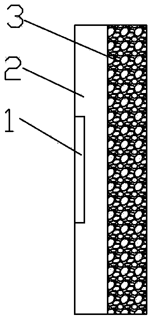
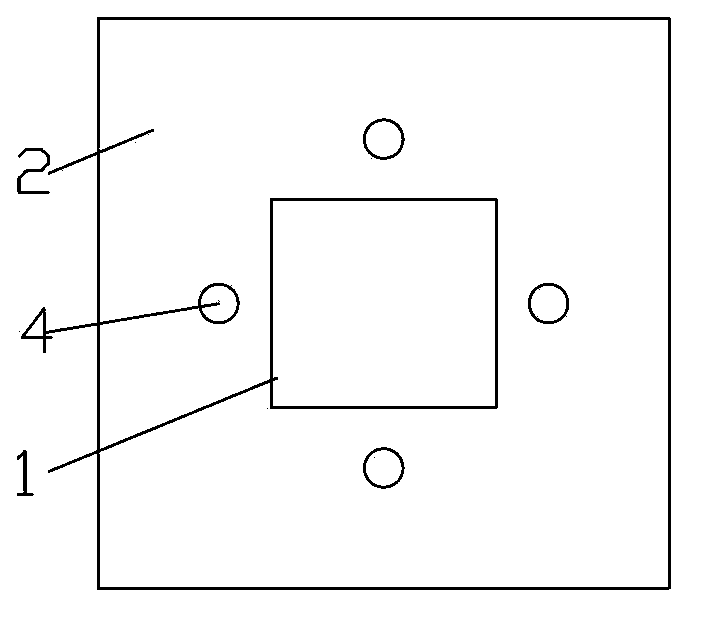
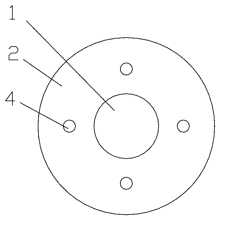
[0086] When the LED chip is 30W, the main structure of the integrated LED light source cooling device adopts a double-layer overlapping structure;
[0087] Material preparation:
[0088] The first layer (i.e. the base):
[0089] Material A: silicon carbide powder (quality 95%, the quality here is the mass content of silicon carbide); fineness 240 mesh;
[0090] Material B: silicon carbide powder fineness 90 mesh;
[0091] Mass ratio: material A: material B=7:3;
[0092] Silica sol [Quality is above 12%. That is, containing more than 12% silicon] is 15% of the total mass of material A and material B.
[0093] The second layer (ie heat sink):
[0094] (1) Material C: silicon carbide powder fineness 80 mesh
[0095] (2) Material D: silicon carbide powder fineness 100 mesh
[0096] Mass ratio: material C: material D=7:3;
[0097] (3) Epoxy resin (mass is 10% of the total mass of material C and material D)
[0098] (4) Pore-forming agent ethyl naphthalene (mass is 3% of th...
example 2
[0104] When the LED chip is 50W, the main structure of the integrated LED light source cooling device adopts a double-layer overlapping structure;
[0105] Material preparation:
[0106] First layer (pedestal):
[0107] (1) Material A: silicon carbide powder (quality 95%) with a fineness of 60 mesh, or use ceramic fiber ceramic particles
[0108] (2) Material B: silicon carbide powder (quality 95%) fineness 100 mesh
[0109] Mass ratio: Material A: Material B=6:4
[0110] (3) Silica sol [the quality is above 12%. That is, containing more than 12% silicon] is 15% of the total mass of material A and material B.
[0111] The second layer (heat sink):
[0112] (1) Material C: silicon carbide powder fineness 30 mesh
[0113] (2) Material D: silicon carbide powder fineness 80 mesh
[0114] Mass ratio: material C: material D=6:4;
[0115] (3) Epoxy resin (mass is 20% of the total mass of material C and material D)
[0116] (4) Pore-forming agent ethyl naphthalene (mass is 1...
example 4
[0122] Step 1: Prepare the base;
[0123] Prepare material A with a fineness of 240 mesh, material B with a fineness of 90 mesh, and silica sol; material A is at least one of silicon carbide powder, ceramic fiber and ceramic particles; material B is silicon carbide powder;
[0124] The mass ratio of material A and material B is 7:3;
[0125] The quality of silica sol is 15% of the total mass of material A and material B;
[0126] Coat the release agent on the first preform mold, put the printed circuit board (0.5-1.5mm thick copper foil thickness) into the first preform mold; use silica sol to mix material A and material B evenly as Die-casting raw materials for die-casting, demoulding after die-casting; pressure range 150-300 N; drying after demoulding, that is, the preparation of the base is completed;
[0127] Step 2: Grinding and packaging:
[0128]There is a packaging groove at the front end of the base (you can also not set the packaging groove, just solder the LED ch...
PUM
 Abstract
Description
Claims
Application Information
 - R&D
- Intellectual Property
- Life Sciences
- Materials
- Tech Scout
- Unparalleled Data Quality
- Higher Quality Content
- 60% Fewer Hallucinations
Browse by: Latest US Patents, China's latest patents, Technical Efficacy Thesaurus, Application Domain, Technology Topic, Popular Technical Reports.
© 2025 PatSnap. All rights reserved.Legal|Privacy policy|Modern Slavery Act Transparency Statement|Sitemap|About US| Contact US: help@patsnap.com


