


Quick Research
Generate reliable direction feasibility study reports for your R&D in just a few steps.

Technical Q&A
Discover and master advanced knowledge NOW. Basics, ideas, possibilities, all at once.

Find Solutions
As an expert in R&D theories, this can generate solutions to your technical problems instantly.

Evaluate Feasibility
Analyze your overall solution with one click, know your potential R&D risks in advance.

Monitor Landscape
Get weekly tech updates, stay abreast of the latest tech innovations and key insights.
Semiconductor device structure and fabrication method thereof
A device structure and semiconductor technology, applied in semiconductor/solid-state device manufacturing, transistors, electrical components, etc., can solve problems such as increased parasitic resistance, limited process selectivity, contact hole and gate short circuit, etc., and achieve the effect of improving performance
- Summary
- Abstract
- Description
- Claims
- Application Information
AI Technical Summary
Problems solved by technology
Method used
Image

Examples
no. 1 example
[0026] The following will refer to the attached Figure 5-10 A first embodiment of the present invention will be described.
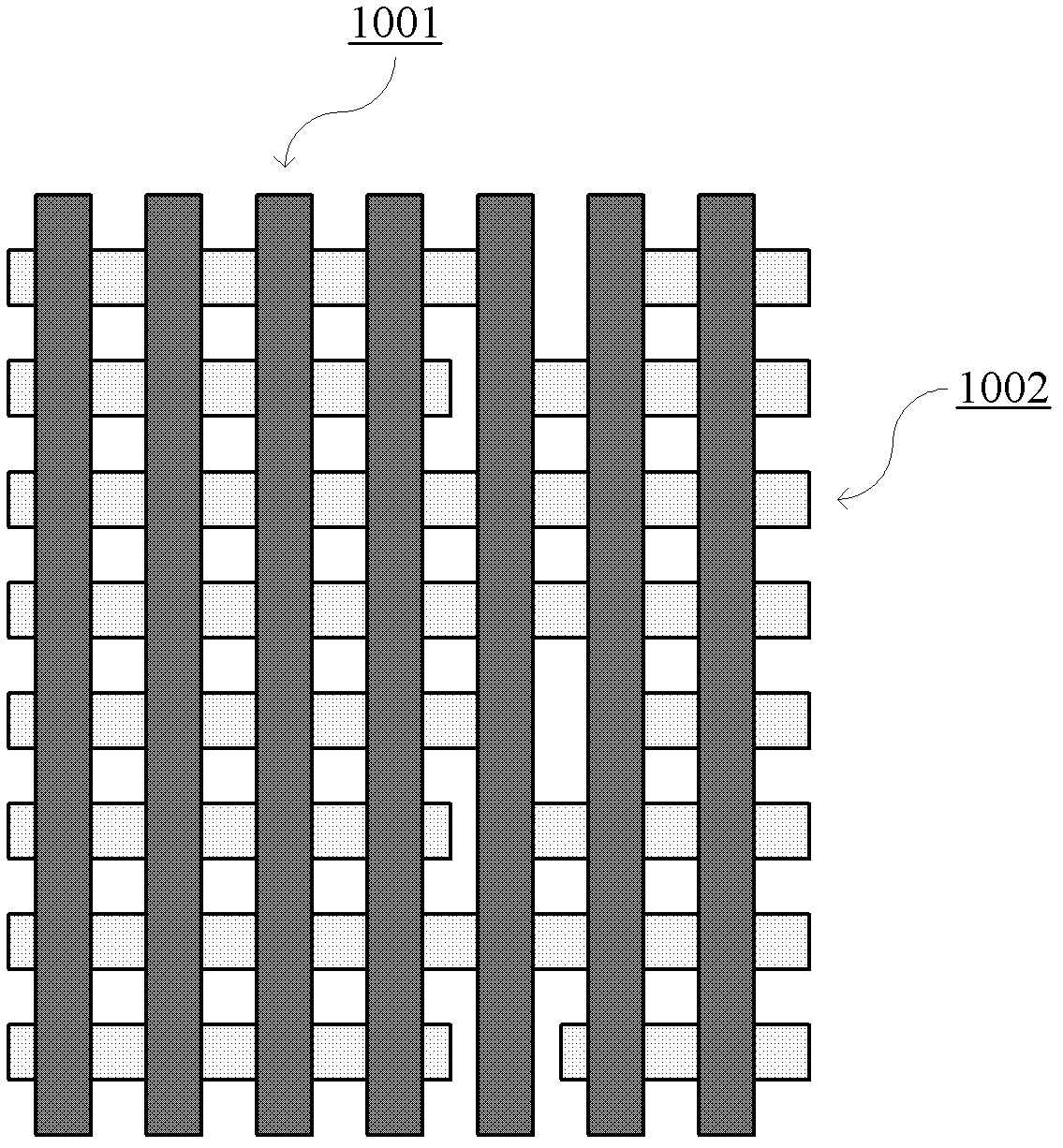
[0027] Figure 5 A portion of a device layout formed on a semiconductor substrate is shown. The semiconductor substrate may include any suitable semiconductor substrate material, specifically, but not limited to, silicon, germanium, silicon germanium, SOI (silicon on insulator), silicon carbide, gallium arsenide, or any III / V compound semiconductor, etc. . The semiconductor substrate may include various doping configurations according to design requirements known in the art (eg p-type substrate or n-type substrate). In addition, the semiconductor substrate may optionally include epitaxial layers, which may be stressed to enhance performance. In the following description, a conventional Si substrate is taken as an example for description.
[0028] An STI (Shallow Trench Isolation) region 3001 and an active region 3002 surrounded by the STI region 30...
no. 2 example
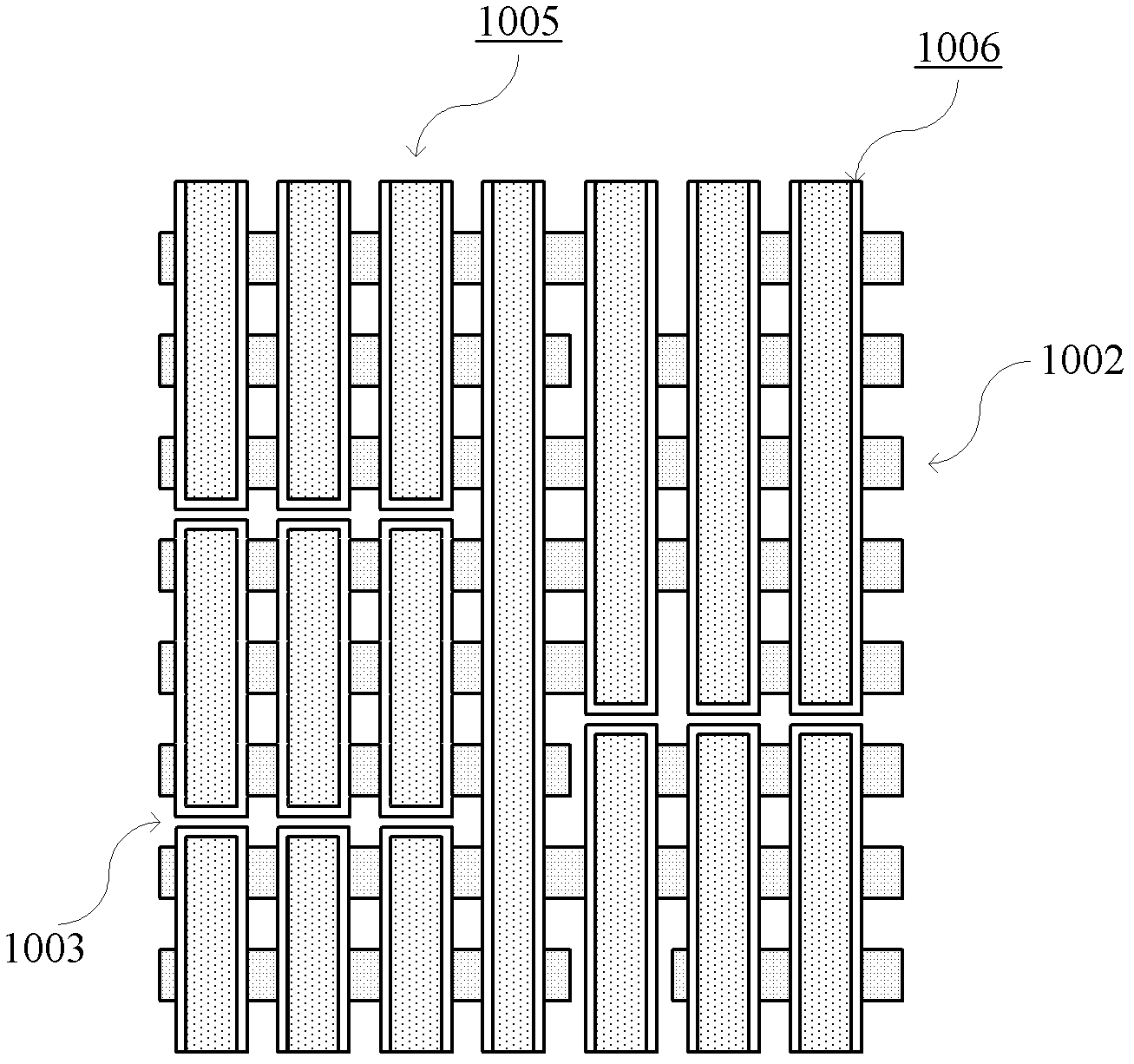
[0061] The method of the present invention is also compatible with replacement gate processes. Below, refer to the attached Figures 11 to 13 A second embodiment of the present invention is described, in which a replacement gate process is combined, that is, a sacrificial gate line is formed first, and then replaced by a replacement gate line.
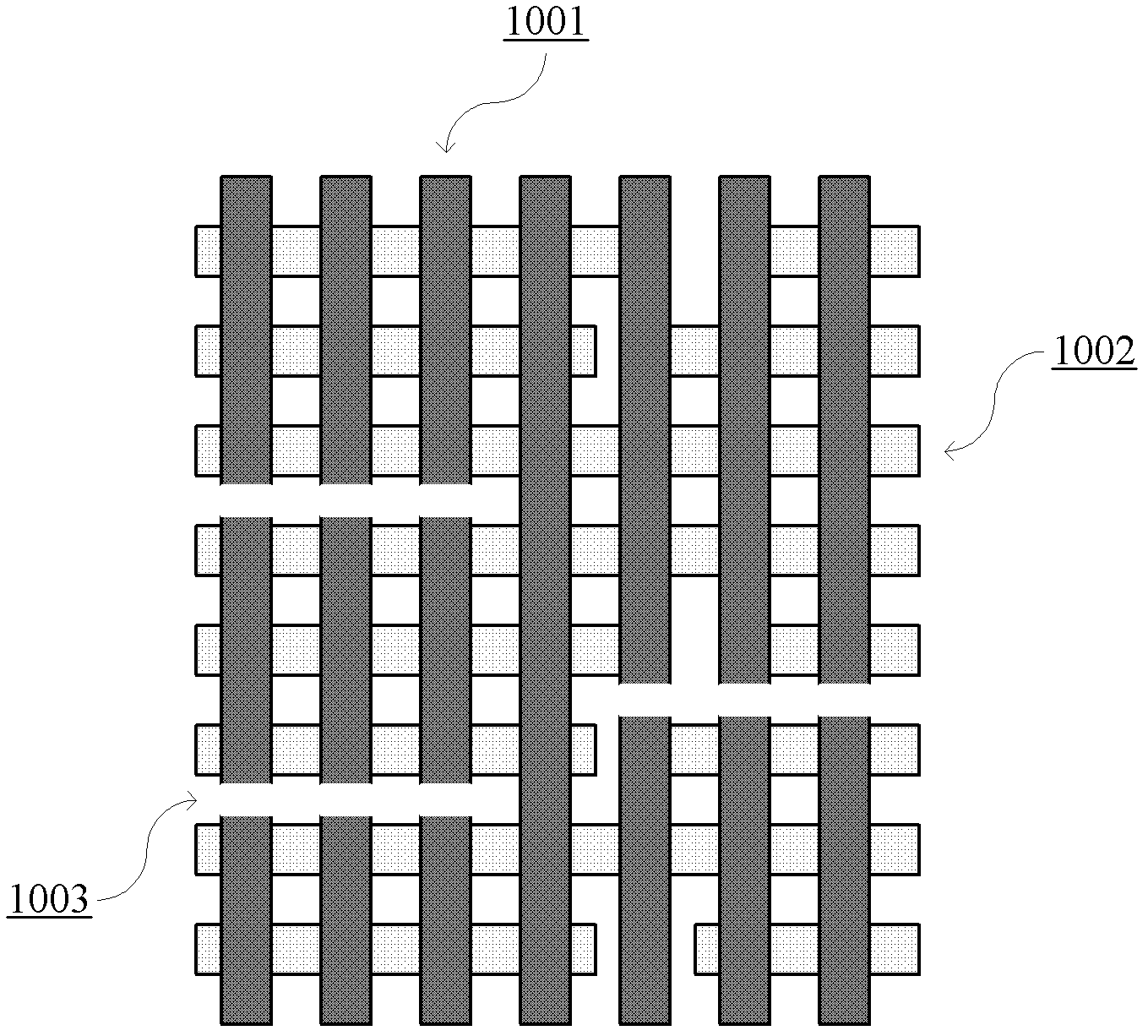
[0062] Hereinafter, the difference between the second embodiment and the first embodiment will be described emphatically, and the same processing will not be repeated. The same reference numerals refer to the same parts in the drawings.
[0063] Such as Figure 11 As shown in (a), as in the first embodiment, a sacrificial gate line 3005 is formed by printing parallel gate line patterns and etching. The sacrificial gate line 3005 is generally formed of polysilicon. Then process according to the conventional process to form a semiconductor device structure, such as forming a source / drain region 3007 in the semiconductor substrate on b...
PUM
 Abstract
Description
Claims
Application Information
 - R&D Engineer
- R&D Manager
- IP Professional
- Industry Leading Data Capabilities
- Powerful AI technology
- Patent DNA Extraction
Browse by: Latest US Patents, China's latest patents, Technical Efficacy Thesaurus, Application Domain, Technology Topic, Popular Technical Reports.
© 2024 PatSnap. All rights reserved.Legal|Privacy policy|Modern Slavery Act Transparency Statement|Sitemap|About US| Contact US: help@patsnap.com