
Touch inductor for capacitive touch screen with film structure and manufacturing method thereof

A technology of touch sensing and structural capacitance, which is applied to the photo-engraving process, instruments, electrical and digital data processing of the pattern surface, etc., can solve the problems of difficult production, high cost, and high requirements for production equipment, and can solve the problem of low pattern accuracy. , The effect of improving product yield and reducing production cost

Active Publication Date: 2013-01-16
TRULY OPTO ELECTRONICS
View PDF4 Cites 7 Cited by
  • Summary
  • Abstract
  • Description
  • Claims
  • Application Information

AI Technical Summary

Problems solved by technology

[0003] The first is the screen printing insulating oil method commonly used in the film structure capacitive touch screen industry. The line width and line spacing of the conductive layer pattern of the touch sensor produced by this method can only be at least 100 microns and 100 microns. Therefore, the linearity of the capacitive touch screen made with this touch sensor is not high, and it is easy to produce false touches. It is not suitable for capacitive touch screens with larger sizes (such as 3.5 inches or above), and the application is limited.
[0004] The second is to use a liquid photoresist coating method similar to the liquid crystal display industry. This method solves the problem of low pattern accuracy of the silk screen method. The line width and line spacing of the touch sensor produced by this method It can reach 40 microns or about 40 microns, so the touch screen made of this touch sensor has a high linearity; however, because the film is soft and easy to bend, it is difficult to apply liquid photoresist on the surface of the conductive film. Uniform coating, using this method to make touch sensors requires high production equipment, low production yield, difficult production and high cost

Method used

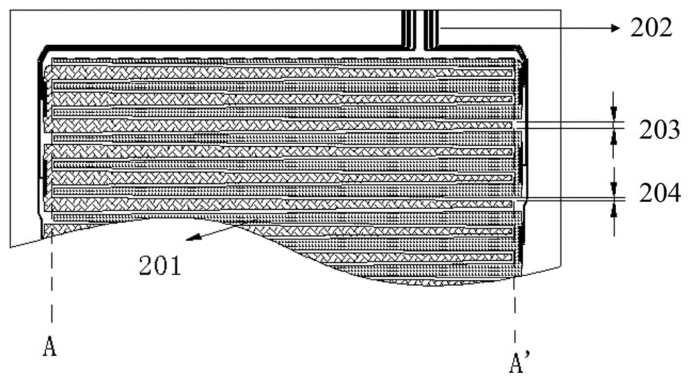

Image

  • Touch inductor for capacitive touch screen with film structure and manufacturing method thereof
  • Touch inductor for capacitive touch screen with film structure and manufacturing method thereof

Examples


Embodiment Construction

[0032] In order to make the above objects, features and advantages of the present invention more comprehensible, specific implementations of the present invention will be described in detail below in conjunction with the accompanying drawings.

[0033] In the following description, a lot of specific details are set forth in order to fully understand the present invention, but the present invention can also be implemented in other ways different from those described here, and those skilled in the art can do it without departing from the meaning of the present invention. By analogy, therefore, the present invention is not limited to the specific examples disclosed below.

[0034] The invention provides a film structure capacitive touch screen touch sensor and a manufacturing method thereof.

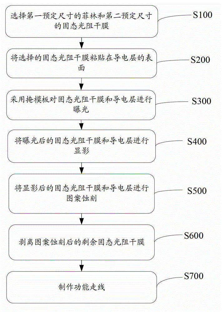
[0035] see figure 1 . figure 1 It is a flow chart of the manufacturing method of the touch sensor of the film structure capacitive touch screen of the present invention, and the manufactu...


PUM


Abstract

The invention provides a touch inductor for a capacitive touch screen with a film structure and a manufacturing method thereof. The manufacturing method comprises the following steps: selecting a film which has a first preset size and comprises a conductive layer and a solid-state light resistance dry film with a second preset size; adhering the solid-state light resistance dry film to the surface of the conductive layer; exposing the solid-state light resistance dry film and the conductive layer by employing a mask plate; developing the exposed solid-state light resistance dry film and the conductive layer; performing pattern etching on the developed solid-state light resistance dry film and the conductive layer; stripping the residual solid-state light resistance dry film subjected to pattern etching; and manufacturing functional routing. According to the manufacturing method, the problem that the method for coating liquid-state light resistance glue is difficult to manufacture is solved, the product performance of a touch screen is improved, the production cost is reduced, and the touch inductor has the advantage of extremely high cost performance.

Description

technical field [0001] The invention relates to the technical field of capacitive touch screens, in particular to a touch sensor of a capacitive touch screen with a film structure and a manufacturing method thereof. Background technique [0002] With the popularization and application of smart phones and tablet computers, more and more attention has been paid to the capacitive touch screen with film structure, and the market prospect is promising. At present, there are two main methods for making the touch sensor of the film structure capacitive touch screen: [0003] The first is the screen printing insulating oil method commonly used in the film structure capacitive touch screen industry. The line width and line spacing of the conductive layer pattern of the touch sensor produced by this method can only be at least 100 microns and 100 microns. Therefore, the linearity of the capacitive touch screen made with this touch sensor is not high, and it is easy to produce false t...

Claims


Application Information

Patent Timeline
IPC IPC(8): G06F3/044G03F7/00
Inventor 苏初榜蔡汉业吕一帆张良何基强李建华
Owner TRULY OPTO ELECTRONICS
Learn More