
Method for grinding silicon chips

A grinding method and technology of silicon wafers, applied in the direction of grinding tools, etc., can solve problems such as low product yield, high grinding cost, and defects, and achieve the effect of high product yield and reduced grinding cost

Inactive Publication Date: 2015-07-01
JINGHUA ELECTRONICS MATERIAL
View PDF0 Cites 6 Cited by
  • Summary
  • Abstract
  • Description
  • Claims
  • Application Information

AI Technical Summary

Problems solved by technology

The grinding process in the prior art uses FO1000 grinding sand, and the grinding cost is high
PWA9 is a kind of grinding sand with a lower price, but when using PWA9 to grind, the grinding will cause more scratches on the surface of the silicon wafer, and the product yield is low
After silicon wafer grinding, the defect rate due to line marks and debris is 1.5%

Method used


Image

  • Method for grinding silicon chips
  • Method for grinding silicon chips

Examples


Embodiment 1

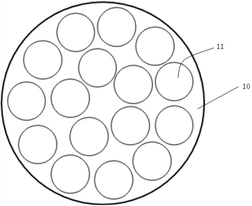
[0014] Silicon wafer grinding methods, such as figure 1 As shown, the silicon wafer is 4 inches, and a 4-inch 16-hole planetary wafer is used to grind the silicon wafer. Sixteen accommodating holes 11 are provided on the planetary plate 1 . The silicon wafer is placed in the holding hole 11 for grinding. Grinding with PWA9 grinding mortar liquid; Grinding separately under multi-stage pressure, the first stage pressure is 270kg, the speed is 5, the speed ratio is 0.5, and the grinding time is 45 seconds; the second stage pressure is 150kg, the speed is 15, and the speed ratio is 0.5. The grinding time is 90 seconds; the pressure of the third stage is 115kg, the speed is 25, the speed ratio is 0.5, and the grinding time is 90 seconds; the pressure of the fourth stage is 100kg, the speed is 30, the speed ratio is 0.5, and the grinding time is 46 seconds; the pressure of the fifth stage is 70kg, speed 35, speed ratio 0.5, grinding time 10 minutes; the interval between pressure c...

Embodiment 2

[0016] Silicon wafer grinding method, the silicon wafer is 4 inches, and a 4-inch 16-hole planetary plate is used to grind the silicon wafer. like figure 1 As shown, the silicon wafer is 4 inches, and a 4-inch 16-hole planetary wafer is used to grind the silicon wafer. Sixteen accommodating holes 11 are provided on the planetary plate 1 . The silicon wafer is placed in the holding hole 11 for grinding. Grinding with PWA9 grinding mortar liquid; Grinding separately under multi-stage pressure, the first stage pressure is 269kg, the speed is 6, the speed ratio is 0.5, and the grinding time is 45 seconds; the second stage pressure is 150kg, the speed is 15, and the speed ratio is 0.4. The grinding time is 90 seconds; the third stage pressure is 123kg, the speed is 24, the speed ratio is 0.6, and the grinding time is 100 seconds; the fourth stage pressure is 95kg, the speed is 35, the speed ratio is 0.5, and the grinding time is 45 seconds; the fifth stage pressure is 75kg, spee...

Embodiment 3

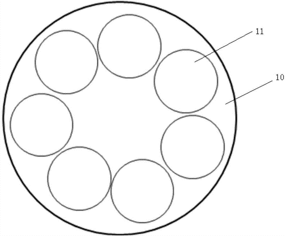
[0018] Silicon wafer grinding methods, such as figure 2 As shown, the silicon wafer is 6 inches, and a 6-inch 7-hole planetary wafer is used to grind the silicon wafer. Seven accommodating holes 11 are arranged on the planet plate 1 . The silicon wafer is placed in the holding hole 11 for grinding. Grinding with PWA9 grinding mortar liquid; Grinding separately under multi-stage pressure, the first stage pressure is 269kg, the speed is 4, the speed ratio is 0.4, and the grinding time is 40 seconds; the second stage pressure is 146kg, the speed is 14, and the speed ratio is 0.5. The grinding time is 80 seconds; the pressure of the third stage is 125kg, the speed is 24, the speed ratio is 0.6, and the grinding time is 100 seconds; the pressure of the fourth stage is 110kg, the speed is 28, the speed ratio is 0.4, and the grinding time is 42 seconds; the pressure of the fifth stage is 80kg, speed of 34, speed ratio of 0.5, grinding time of 9 minutes; the interval between pressu...


PUM


Abstract

The invention discloses a method for grinding silicon chips. The method is characterized in that the silicon chips are ground by the aid of PWA9 grinding sand slurry; the silicon chips are respectively ground under multilevel pressures, the first-level pressures range from 265kg to 275kg, the rotational speeds range from 4 revolutions / min to 6 revolutions / min, rotational speed ratios range from 0.4 to 0.6, and the grinding time ranges from 40 seconds to 50 seconds; the second-level pressures range from 140kg to 160kg, the rotational speeds range from 14 revolutions / min to 16 revolutions / min, rotational speed ratios range from 0.4 to 0.6, and the grinding time ranges from 60 seconds to 120 seconds; the third-level pressures range from 110kg to 120kg, the rotational speeds range from 24 revolutions / min to 26 revolutions / min, rotational speed ratios range from 0.4 to 0.6, and the grinding time ranges from 60 seconds to 120 seconds; the fourth-level pressures range from 90kg to 110kg, the rotational speeds range from 28 revolutions / min to 32 revolutions / min, rotational speed ratios range from 0.4 to 0.6, and the grinding time ranges from 40 seconds to 50 seconds; the fifth-level pressures range from 65kg to 75kg, the rotational speeds range from 34 revolutions / min to 36 revolutions / min, rotational speed ratios range from 0.4 to 0.6, and the grinding time ranges from 9min to 11min; the various levels of pressures are switched over at time intervals which range from 5 seconds to 15 seconds. The method for grinding the silicon chips has the advantages that the silicon chips are ground by the aid of PWA9 grinding sand, and accordingly the grinding cost can be reduced by 10%; ground products are high in yield, and the defect rate due to saw marks and fragments can be reduced and reaches 0.5%.

Description

technical field [0001] The invention relates to a silicon wafer grinding method. Background technique [0002] Wafer grinding is an important process in the production of silicon wafers. The grinding process in the prior art uses FO1000 grinding sand, and the grinding cost is high. PWA9 is a kind of grinding sand with a lower price, but when using PWA9 for grinding, the grinding will cause more scratches on the surface of the silicon wafer, and the product yield will be low. After the silicon wafer is ground, the defect rate due to line marks and debris is 1.5%. Contents of the invention [0003] The object of the present invention is to provide a silicon wafer grinding method with low grinding cost in order to overcome the deficiencies in the prior art. [0004] To achieve the above object, the present invention is achieved through the following technical solutions: [0005] The silicon wafer grinding method is characterized in that it is ground with PWA9 grinding mor...

Claims


Application Information

Patent Timeline
IPC IPC(8): B24B1/00B24B37/16
CPCB24B1/00B24B37/16
Inventor 沈辉辉黄春峰邹晓明陈建纲刘苏生
Owner JINGHUA ELECTRONICS MATERIAL
Learn More