Insulated gate bipolar transistor terminal and producing method thereof
A bipolar transistor and insulated gate technology, applied in semiconductor/solid-state device manufacturing, semiconductor devices, electrical components, etc., can solve the problems of increasing chip manufacturing costs, large chips, and large total chip area, so as to reduce the total area, Reduce the area and eliminate the effect of electric field concentration
- Summary
- Abstract
- Description
- Claims
- Application Information
AI Technical Summary
Problems solved by technology
Method used
Image
Examples
Embodiment 1
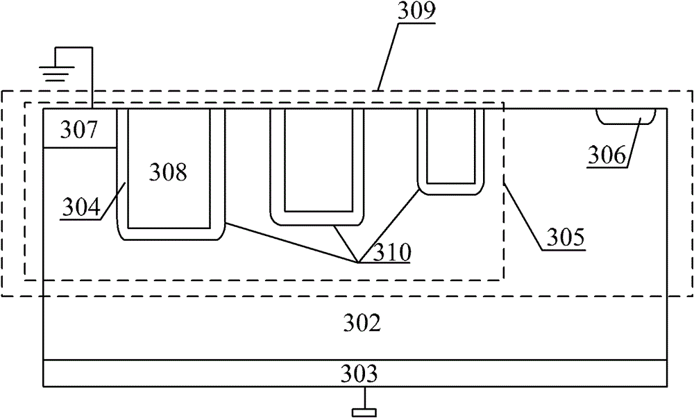
[0036] refer to figure 2 , figure 2 A schematic structural diagram of an IGBT terminal provided by an embodiment of the present invention, the IGBT terminal includes: a drift region 302; a terminal protection structure 309 located in the front of the drift region 302; within the collector region 303 . The drift region 302 is a lightly doped semiconductor of the first conductivity type, and the collector region 303 is a heavily doped semiconductor of the second conductivity type. In this embodiment, the doping type of the semiconductor of the first conductivity type is opposite to that of the semiconductor of the second conductivity type.
[0037] The terminal protection structure 309 includes: a voltage division protection area 305 of the inner ring and a cut-off ring 306 of the outer ring; wherein, the voltage division protection area 305 of the inner ring includes: a main junction 307 and a voltage division groove 310, the The voltage dividing trench 310 is located on t...
Embodiment 2
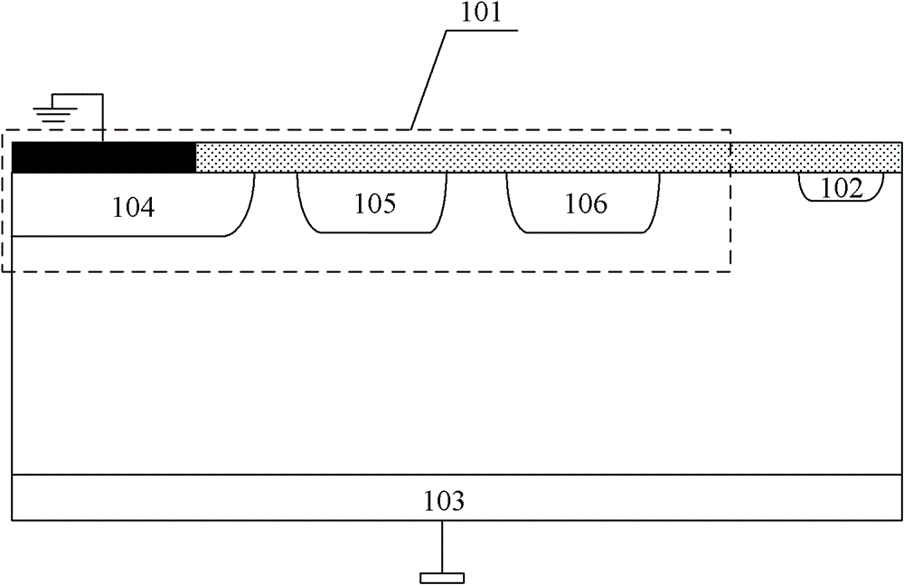
[0044] In the background art, the IGBT terminal protection structure is described in detail as a field-limiting ring (FLR) structure. In addition to the disadvantage of occupying a large proportion of the total chip area, the field-limiting ring structure is also extremely vulnerable to interface instability. and oxide layer ( figure 1 Part of the interfacial charge on the midlimit ring, which in turn affects the breakdown voltage of the device and the reliability under high voltage.
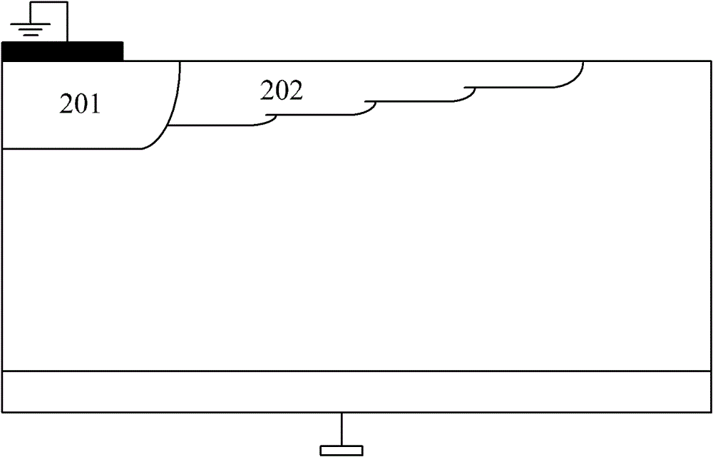
[0045] Furthermore, in addition to the field limiting ring structure being susceptible to surface charges, the Junction Termination Extension (JTE) structure also suffers from this disadvantage. refer to image 3 , image 3 is a schematic diagram of a junction terminal extension (JTE) structure in a conventional IGBT device, showing a heavily doped main junction 201 and a lightly doped junction near the main junction 201 formed by ion implantation or diffusion process Partial pressure area 202 ...
Embodiment 3
[0053] The terminal of the IGBT provided by the present invention has been described in detail above, and the manufacturing method of the terminal will be described in detail below.
[0054] refer to Figure 5 , Figure 5 It is a schematic flowchart of a method for manufacturing an insulated gate bipolar transistor terminal provided by an embodiment of the present invention. The method specifically includes the following steps:
[0055] Step S1: using a lightly doped silicon substrate as a drift region.
[0056] The existing lightly doped silicon substrate is used as the drift region for manufacturing the IGBT terminal, and the subsequent process steps are all realized in the silicon substrate or on the silicon substrate.
[0057] Step S2: forming a terminal protection structure in the drift region; wherein, the terminal protection structure includes: a main junction, a stop ring, and a voltage dividing trench between the main junction and the stop ring.
[0058] This step ...
PUM
 Abstract
Description
Claims
Application Information
 - R&D
- Intellectual Property
- Life Sciences
- Materials
- Tech Scout
- Unparalleled Data Quality
- Higher Quality Content
- 60% Fewer Hallucinations
Browse by: Latest US Patents, China's latest patents, Technical Efficacy Thesaurus, Application Domain, Technology Topic, Popular Technical Reports.
© 2025 PatSnap. All rights reserved.Legal|Privacy policy|Modern Slavery Act Transparency Statement|Sitemap|About US| Contact US: help@patsnap.com


