


Quick Research
Generate reliable direction feasibility study reports for your R&D in just a few steps.

Technical Q&A
Discover and master advanced knowledge NOW. Basics, ideas, possibilities, all at once.

Find Solutions
As an expert in R&D theories, this can generate solutions to your technical problems instantly.

Evaluate Feasibility
Analyze your overall solution with one click, know your potential R&D risks in advance.

Monitor Landscape
Get weekly tech updates, stay abreast of the latest tech innovations and key insights.
Semiconductor chip
A semiconductor and chip technology, applied in the direction of semiconductor devices, semiconductor/solid-state device components, electric solid-state devices, etc., can solve the problems of limited number and value of on-chip decoupling capacitors, small parasitic inductance, etc.
- Summary
- Abstract
- Description
- Claims
- Application Information
AI Technical Summary
Problems solved by technology
Method used
Image


Examples
Embodiment 1
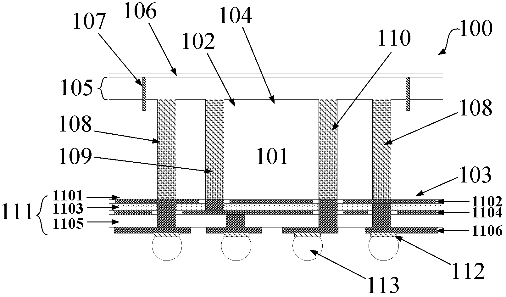
[0111] refer to figure 1 , which shows a schematic cross-sectional view of the semiconductor chip 100 . The semiconductor chip 100 includes a semiconductor substrate 101 and a plurality of conductive TSVs penetrating the semiconductor substrate. A circuit area 104 (such as transistors, diodes, not shown in the figure) is disposed on the front surface 102 of the semiconductor substrate 101 . A seal ring 107 surrounds the circuit area 104 of the semiconductor chip, and its main function is to prevent mechanical damage to the chip during dicing, and at the same time shield external electromagnetic interference. A metal wiring layer 105 is disposed on the circuit area 104 . The metal wiring layer 105 includes at least one layer of metal wiring, and adjacent layers of metal wiring are separated by dielectric material layers (not shown in the figure). At present, the commonly used dielectric material is silicon dioxide. In order to reduce the parasitic capacitance, crosstalk, and...
Embodiment 2
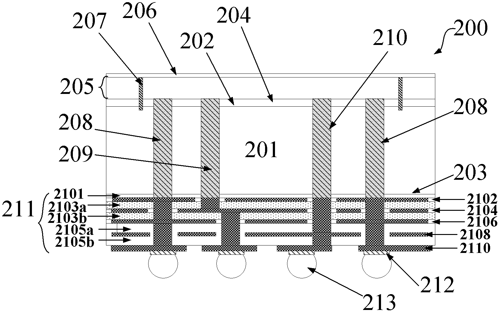
[0121] figure 2 It is a schematic cross-sectional view of the semiconductor chip 200, the conductive through-silicon vias (TSVs) penetrating the semiconductor substrate 201 (including ground through-silicon vias (Ground TSV) 208, power supply through-silicon vias (Power TSV) 209 and signal through-silicon vias (Signal through-silicon vias). TSV) 210) form an electrical connection of the metal wiring in the metal wiring layer 205 of the semiconductor chip to the backside surface 203 of the semiconductor substrate. That is, conductive through-silicon vias (TSVs) penetrating the semiconductor substrate 201 form an electrical connection from one side of the semiconductor chip 200 to the opposite side. The metal layers 2102, 2104, 2106, 2108, and 2110 located on the back passivation layer 2101 of the semiconductor substrate are arranged in sequence, and the spaces between the metal layer 2102 and the metal layer 2104, and between the metal layer 2104 and the metal layer 2106 are r...
Embodiment 3
[0125] Explain the situation that a semiconductor chip requires two or more voltages for power supply due to functional and performance requirements, for example, two or more voltages are required to supply power to different functional areas of the semiconductor chip. The values (volts) of these two or more power supply voltages may be the same or different. That is to say, different functional regions of the semiconductor chip may require power supplies of different voltage levels (different voltage values), for example: 5V, 3.3V, 1.8V, 1.2V and so on. It is also possible that although different functional areas of the semiconductor chip require the same power supply voltage level (voltage value), the signal types of different functional areas are different, for example: digital signal area, analog signal area, microwave radio frequency signal area, low-speed signal area , high-speed signal area, etc. The power supplies of different functional areas need to be isolated to...
PUM
 Abstract
Description
Claims
Application Information
 - R&D Engineer
- R&D Manager
- IP Professional
- Industry Leading Data Capabilities
- Powerful AI technology
- Patent DNA Extraction
Browse by: Latest US Patents, China's latest patents, Technical Efficacy Thesaurus, Application Domain, Technology Topic, Popular Technical Reports.
© 2024 PatSnap. All rights reserved.Legal|Privacy policy|Modern Slavery Act Transparency Statement|Sitemap|About US| Contact US: help@patsnap.com