Eureka AIR delivers breakthrough ideas for toughest innovation challenges, trusted by R&D personnel around the world.

Spread method of polycrystalline silicon solar cell

A technology of a solar cell and a diffusion method, which is applied in the field of solar cell manufacturing, can solve the problems of low impurity concentration at the center point of a silicon wafer, low photoelectric conversion efficiency of a cell, poor diffusion uniformity, etc., and achieves improved photoelectric conversion efficiency and uniform impurity concentration distribution. , the effect of uniform distribution

Inactive Publication Date: 2012-12-12
JIANGYIN XINHUI SOLAR ENERGY
View PDF6 Cites 41 Cited by
  • Summary
  • Abstract
  • Description
  • Claims
  • Application Information

AI Technical Summary

Problems solved by technology

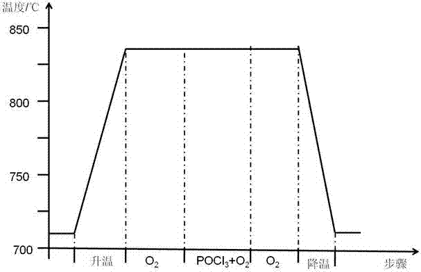
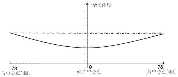
Due to the small distance between silicon wafers in the diffusion furnace tube (about 2.5mm), it is difficult to obtain the same amount of phosphorus source at the center of the silicon wafer as the surrounding, resulting in poor diffusion uniformity, low impurity concentration at the center of the silicon wafer, and square resistance. On the high side, the final photoelectric conversion efficiency of the cell is low
It is difficult to change this problem simply by changing the temperature, concentration or time, and the degree of optimization is limited

Method used


Image

  • Spread method of polycrystalline silicon solar cell
  • Spread method of polycrystalline silicon solar cell
  • Spread method of polycrystalline silicon solar cell

Examples


Embodiment Construction

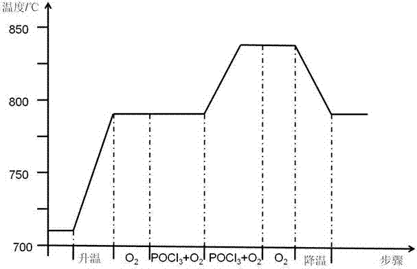
[0055] See figure 2 , The invention relates to a polycrystalline silicon solar cell diffusion method, and the process steps of the diffusion method are as follows:

[0056] Step one, enter the boat

[0057] The silicon wafers after texturing enter the diffusion furnace with an initial temperature of 500~770℃, and the time of entering the boat is 700~900s. During the process of feeding the silicon wafers into the boat, large nitrogen is introduced into the gas inlet pipe of the diffusion furnace, and the flow of large nitrogen is 23500 ~24500sccm.

[0058] Step two, heating up

[0059] The diffusion furnace is heated to 770~790°C, the heating time is 700~900s, and the large nitrogen is introduced during the heating process, and the large nitrogen flow rate is 23500~24500sccm.

[0060] Step three, oxidation

[0061] Keep the temperature of the diffusion furnace at 770~790℃, and pass large nitrogen and oxygen into the diffusion furnace. The flow rate of large nitrogen is 23500~24500sccm, ...


PUM


Abstract

The invention relates to a spread method of a polycrystalline silicon solar cell. The spread method is characterized in that the spread method comprises the following processing steps of entering a boat, warming, oxidizing, spreading, redistributing, cooling and going out the boat, wherein the spreading step comprises low temperature pre-deposition and then high temperature spreading. Reaction between a phosphorus source and a silicon wafer cannot be completed under low temperature, so that the low temperature pre-deposition is carried out on low temperature source communication at a first step of spreading, the phosphorus source cannot spread (or conduct spreading with low rate) inside a silicon wafer, the phosphorus source only accumulates on the surface of the silicon wafer, and a phosphorus film with certain thickness is formed on the surface of the silicon wafer after source communication for certain time; and the high temperature spreading is carried out on high temperature source communication at a second step, phosphorus on the surface of an original silicon wafer is reacted with the silicon wafer and spreads to the inside of the silicon wafer, and spreading rates of the center point and the periphery of the silicon wafer are same. Therefore, spreading uniformity is good, concentration distribution of impurities on the surface of the silicon wafer and inside the silicon wafer body is even, sheet resistance uniformity is improved, and final photoelectric conversion efficiency of a cell sheet is improved accordingly.

Description

Technical field [0001] The invention relates to a diffusion method of a polycrystalline silicon solar cell, belonging to the field of solar cell manufacturing. Background technique [0002] Solar cell is a device that directly converts light energy into electrical energy. Because of its cleanness, non-polluting, inexhaustible and inexhaustible use, it has received more and more attention. [0003] The diffusion of polycrystalline silicon solar cells is usually made by phosphorus diffusion. This step is a key step in the entire preparation process. Its quality will directly affect the photovoltaic conversion efficiency of the battery. The typical junction preparation is divided into two steps: the first step is to pass through with nitrogen. Liquid Phosphorus Oxychloride (POCl 3 ), the required impurity (phosphorus) is transported to the surface of the high temperature silicon wafer with carrier gas nitrogen (N2), and the impurity diffusion depth is about hundreds of nanometers; the...

Claims


Application Information

Patent Timeline
Patent Type & Authority Applications(China)
IPC IPC(8): H01L31/18H01L21/223C30B31/06
CPCY02P70/50
Inventor 赵贵燕邱军辉王世贤龚丽坤
Owner JIANGYIN XINHUI SOLAR ENERGY
Why Eureka
Eureka Blog
Learn More