Bi-polycrystal SOI (Silicon On Insulator) Bi CMOS (Complementary Metal Oxide Semiconductor) integrated device with SiGe clip-shaped channel and preparation method thereof

An integrated device, dual polycrystalline technology, applied in semiconductor/solid-state device manufacturing, electrical solid-state devices, semiconductor devices, etc., can solve the problems of oxide layer breakdown, large influence, and inability to further reduce device size.

Inactive Publication Date: 2012-10-10
XIDIAN UNIV
View PDF3 Cites 1 Cited by
  • Summary
  • Abstract
  • Description
  • Claims
  • Application Information

AI Technical Summary

Problems solved by technology

[0005] As the feature size of the device enters the sub-50nm stage, many difficulties are encountered in the research process of the strained Si / SiGe CMOS planar structure: short channel effects, hot carrier effects, etc. make the device size unable to be further reduced; gate oxidation The thinning of the layer thickness leads to the breakdown of the oxide layer, and the tunneling current causes the threshold voltage to drift; the polysilicon depletion effect and the resistance of the polysilicon have an increasing influence on the threshold voltage, etc., all of which make the device and circuit performance unable to continue according to Moore. As the law of development continues to develop, it becomes more important to study devices with new structures.

Method used


Image

  • Bi-polycrystal SOI (Silicon On Insulator) Bi CMOS (Complementary Metal Oxide Semiconductor) integrated device with SiGe clip-shaped channel and preparation method thereof

Examples


Embodiment 1

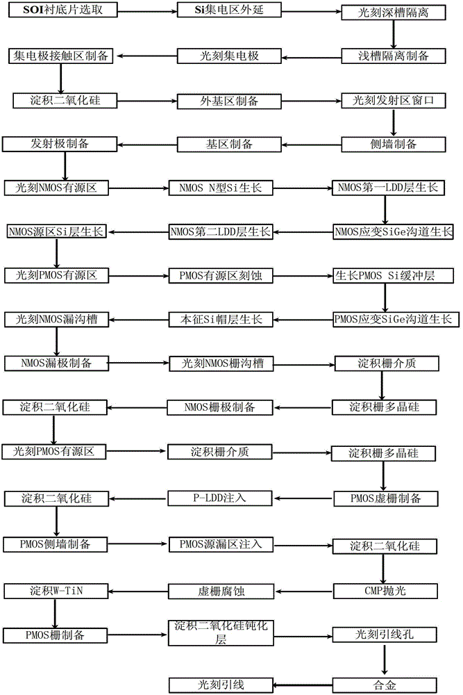
[0127] Example 1: Preparation of a dual poly SOI, strained SiGe back-channel BiCMOS integrated device and circuit based on a self-aligned process with a conductive channel of 45 nm. The specific steps are as follows:

[0128] Step 1, epitaxial growth.

[0129] (1a) Select an SOI substrate, the lower support material of the substrate is Si, and the middle layer is SiO 2 , The thickness is 400nm, the upper layer material is doping concentration is 1×10 17 cm -3 N-type Si with a thickness of 150nm;

[0130] (1b) Using chemical vapor deposition (CVD) method, at 750℃, grow a layer of N-type epitaxial Si layer with a thickness of 100nm on the upper Si material as a collector area, the doping concentration of this layer is 1× 10 17 cm -3 .

[0131] Step 2. The realization method of isolation area preparation is:

[0132] (2a) Using chemical vapor deposition (CVD), at 800℃, deposit a layer of SiO with a thickness of 500nm on the surface of the epitaxial Si layer 2 Floor;

[0133] (2b) In the li...

Embodiment 2

[0200] Embodiment 2: Preparation of a self-aligned double poly SOI, strained SiGe back-channel BiCMOS integrated device and circuit with a 30nm conductive channel, and the specific steps are as follows:

[0201] Step 1, epitaxial growth.

[0202] (1a) Select an SOI substrate, the lower support material of the substrate is Si, and the middle layer is SiO 2 , The thickness is 300nm, the upper material is doping concentration is 5×10 16 cm -3 N-type Si with a thickness of 120nm;

[0203] (1b) Using the chemical vapor deposition (CVD) method, at 700℃, grow a layer of N-type epitaxial Si with a thickness of 80nm on the upper Si material as a collector area, the doping concentration of this layer is 5× 10 16 cm -3 .

[0204] Step 2. Preparation of isolation area.

[0205] (2a) Using chemical vapor deposition (CVD) method, at 700℃, deposit a layer of SiO with a thickness of 400nm on the surface of the epitaxial Si layer 2 Floor;

[0206] (2b) In the lithographic isolation area, a deep groove w...

Embodiment 3

[0273] Embodiment 3: Preparation of a self-aligned double poly SOI, strained SiGe back-channel BiCMOS integrated device and circuit with a 22nm conductive channel, and the specific steps are as follows:

[0274] Step 1, epitaxial growth.

[0275] (1a) Select an SOI substrate, the lower support material of the substrate is Si, and the middle layer is SiO 2 , The thickness is 150nm, the upper layer material is doping concentration is 1×10 16 cm -3 N-type Si with a thickness of 100nm;

[0276] (1b) Using chemical vapor deposition (CVD) method, at 600℃, grow a layer of N-type epitaxial Si with a thickness of 50nm on the upper Si material as a collector area, the doping concentration of this layer is 1× 10 16 cm -3 .

[0277] Step 2. Preparation of isolation area.

[0278] (2a) Using chemical vapor deposition (CVD), at 600℃, deposit a layer of SiO with a thickness of 300nm on the surface of the epitaxial Si layer 2 Floor;

[0279] (2b) In the lithographic isolation area, a deep groove with a...


PUM

PropertyMeasurementUnit
Thicknessaaaaaaaaaa
Thicknessaaaaaaaaaa
Thicknessaaaaaaaaaa

Abstract

The invention discloses a bi-polycrystal SOI (Silicon On Insulator) Bi CMOS (Complementary Metal Oxide Semiconductor) integrated device with a SiGe clip-shaped channel and a preparation method of the device. The preparation method comprises the steps of conducting epitaxy on a collector region of a bipolar device on an SOI substrate, preparing a deep-trench isolator, a base window and base polycrystal, conducting epitaxy on a SiGe base region and a Poly-Si emitter region to form a SiGe HBT (Heterojuntion Bipolar Transistor) device; conducting photoetching on an active region of an NMOS (N-Channel Metal Oxide Semiconductor) device, growing five layers of materials on the region in an epitaxial manner to form the active region of the NMOS device so as to prepare an NMOS device; conducting photoetching on an active region of a PMOS (P-Channel Metal Oxide Semiconductor) device, growing three layers of materials in an epitaxial manner in the region to form the active region of the PMOS device, preparing a virtual grid electrode, and injecting by utilizing a self alignment process so as to form the drain electrode and the source electrode of the PMOS device; etching a virtual grid to prepare the PMOS device, and thus forming the Bi CMOS integrated with a conducting channel being 22-45nm and a circuit of an MOS (Metal Oxide Semiconductor) device, wherein the device and the circuit are based on the self alignment process. According to the preparation method, the self alignment process is adopted, and the characteristic of the anisotropism of the mobility ratio of strain SiGe material is utilized sufficiently, so that a bi-polycrystal SOI strain Bi COMOS integrated circuit with SiGe clip-shaped channel is prepared, and the performance of the circuit is enhanced.

Description

Technical field [0001] The invention belongs to the technical field of semiconductor integrated circuits, and in particular relates to a dual polycrystalline SOI strained SiGe back-channel BiCMOS integrated device and a preparation method. Background technique [0002] Semiconductor integrated circuits are the foundation of the electronics industry, and people's huge demand for the electronics industry promotes the rapid development of this field. In the past few decades, the rapid development of the electronics industry has had a huge impact on social development and the national economy. At present, the electronics industry has become the world's largest industry, occupying a large share of the global market, and its output value has exceeded US$1,000 billion. [0003] Si CMOS integrated circuits have the advantages of low power consumption, high integration, low noise and high reliability, and occupy a dominant position in the semiconductor integrated circuit industry. However...

Claims


Application Information

Patent Timeline
IPC IPC(8): H01L27/12H01L21/84H01L21/8249
Inventor 宋建军胡辉勇吕懿宣荣喜张鹤鸣李妤晨舒斌郝跃
Owner XIDIAN UNIV
Why Eureka
Try Eureka