Manufacturing method of MOS (Metal Oxide Semiconductor) transistor structure integrated with resistive random access memory

A technology of resistive variable memory and manufacturing method, which is applied in semiconductor/solid-state device manufacturing, electric solid-state devices, semiconductor devices, etc., and can solve the problem of complex integrated process of resistive variable memory and MOS transistor, which is unfavorable for the development of the direction of miniaturization of process integrated devices and other problems, to achieve the effect of simple process steps

Inactive Publication Date: 2012-10-03
FUDAN UNIV
View PDF7 Cites 9 Cited by
  • Summary
  • Abstract
  • Description
  • Claims
  • Application Information

AI Technical Summary

Problems solved by technology

[0007] As mentioned above, the integration process of resistive memory and MOS transistors is complicated, which is not conducive to process integration and the development of devices in the direction of miniaturization

Method used


Image

  • Manufacturing method of MOS (Metal Oxide Semiconductor) transistor structure integrated with resistive random access memory
  • Manufacturing method of MOS (Metal Oxide Semiconductor) transistor structure integrated with resistive random access memory
  • Manufacturing method of MOS (Metal Oxide Semiconductor) transistor structure integrated with resistive random access memory

Examples


Embodiment Construction

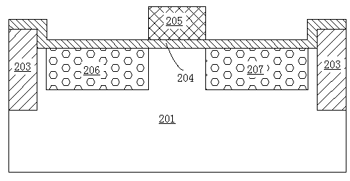
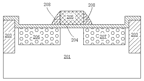
[0022] The present invention will be further described in detail below in conjunction with the accompanying drawings and specific embodiments. In the drawings, for the convenience of illustration, the thicknesses of layers and regions are enlarged or reduced, and the sizes shown do not represent actual sizes. Although these figures do not fully reflect the actual size of the device, they still completely reflect the mutual positions between the regions and the constituent structures, especially the upper-lower and adjacent relationships between the constituent structures.

[0023] The following describes the process flow of an embodiment of preparing the n-type MOS transistor structure of the integrated resistive memory by adopting the method for integrating the resistive memory and the MOS transistor disclosed in the present invention. Figure 4-11 The process of a part of an integrated circuit composed of the devices disclosed in the present invention is described, taking a s...


PUM


Abstract

The invention belongs to the technical field of semiconductor memories below 20nmm and more particularly relates to a manufacturing method of an MOS (Metal Oxide Semiconductor) transistor structure integrated with a resistive random access memory. According to the manufacturing method disclosed by the invention, a source region and a drain region of the MOS transistor are formed by a self-aligned technology, a high-quality gate dielectric layer of the MOS transistor and a resistive random access memory layer of the resistive random access memory are deposited by a primary atomic layer deposition process, and the resistive random access memory and the MOS transistor are integrated together on the premise of not increasing extra process steps. The manufacturing method disclosed by the invention can be compatible with a shallow trench isolation process, or a field oxide layer isolation process and a source/drain ion implantation or diffusion process, is simple in process steps and provides convenience for process integration and devices to develop towards a miniaturization direction.

Description

technical field [0001] The invention belongs to the technical field of semiconductor memory below 20 nanometers, and in particular relates to a method for manufacturing a field effect transistor structure of an integrated resistive variable memory. Background technique [0002] The resistance value of the resistive memory layer of the resistive memory has two different states of high resistance state and low resistance state under the action of an applied voltage, which can be used to represent two states of "0" and "1" respectively. Under different applied voltage conditions, the resistance value of the RRAM can be reversibly switched between a high-resistance state and a low-resistance state, so as to realize information storage. Resistive memory has the advantages of simple preparation, high storage density, low operating voltage, fast read and write speed, long retention time, non-destructive read, low power consumption, and traditional CMOS (that is, complementary metal...

Claims


Application Information

Patent Timeline
Patent Type & Authority Applications(China)
IPC IPC(8): H01L21/336H01L27/24
Inventor 林曦王鹏飞孙清清张卫
Owner FUDAN UNIV
Why Eureka
Try Eureka