Semiconductor structure with low resistance substrate and low power loss

A semiconductor and conductive structure technology, applied in semiconductor devices, semiconductor/solid-state device manufacturing, semiconductor/solid-state device components, etc., can solve problems such as micro-cracking, product service life reduction, cost increase, etc., to achieve continuous production capacity and reduce Effect of power loss and resistance reduction

Inactive Publication Date: 2012-08-29
NIKO SEMICON
View PDF5 Cites 2 Cited by
  • Summary
  • Abstract
  • Description
  • Claims
  • Application Information

AI Technical Summary

Problems solved by technology

The traditional method of reducing the resistance of the substrate uses chip thinning technology to mechanically thin the power metal oxide semiconductor chip from about 300 microns (μm) to about 50 μm. figure 2 As shown in the vertical power metal oxide semiconductor structure with a thinned substrate, the thinned chip is then subjected to subsequent semiconductor packaging processes. However, such a thin chip will greatly increase the probability of fragmentation during the subsequent process and transportation process. In order to protect such a thin chip, in each process, it is necessary to add additional processing procedures and equipment to protect the chip from cracking, resulting in a significant increase in cost
Furthermore, in the packaging and bonding process, the chip must withstand instantaneous stress. Such a thin chip is prone to the potential risk of micro-cracks, resulting in a significant reduction in the usable life of the product.

Method used


Image

  • Semiconductor structure with low resistance substrate and low power loss
  • Semiconductor structure with low resistance substrate and low power loss
  • Semiconductor structure with low resistance substrate and low power loss

Examples


Embodiment Construction

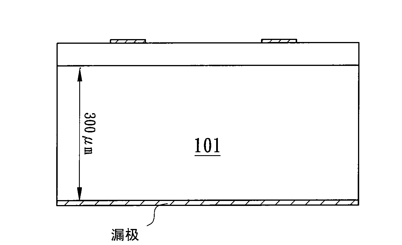
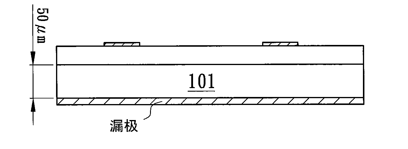
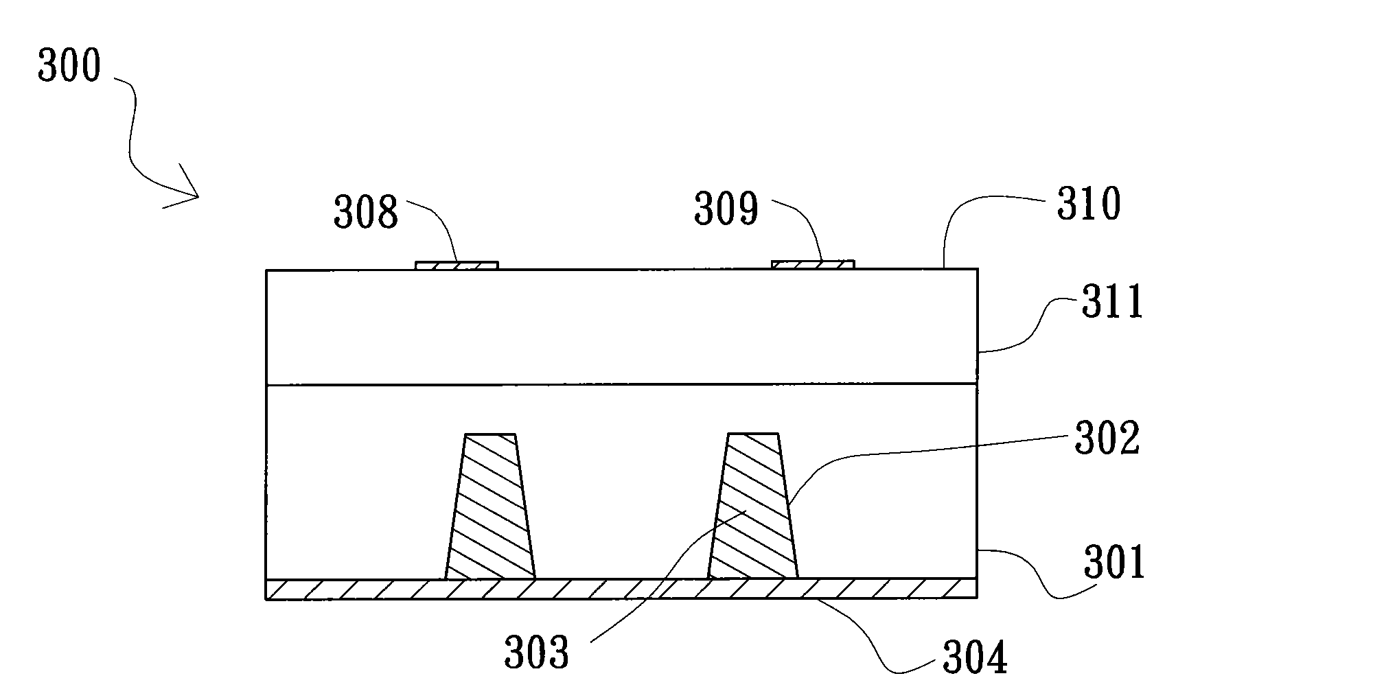
[0038] Figure 3A A first embodiment of the low power loss semiconductor structure of the present invention is shown. Such as Figure 3A As shown, a semiconductor unit 300 has a substrate 301, and at least one hole 302 is formed in the substrate 301, wherein the hole 302 can be implemented in a through silicon via (TSV) manner. A conductive substance 303 is located in the hole 302 , and a conductive structure 304 is located on the surface of the substrate 301 and the conductive substance 303 . The conductive structure 304 serves as a drain electrode of the power semiconductor. A source electrode 308 and a gate electrode 309 are located on a surface 310 of the semiconductor unit 300 . The advantage of reducing the resistance of the semiconductor unit 300 can be achieved by using the conductive structure 304 in the hole 302 to partially or completely replace the substrate 301 with a relatively high resistance value.

[0039] Figure 3B to Figure 3C It is the manufacturing m...


PUM


Abstract

The invention provides a semiconductor structure with a low resistance substrate and low power loss. The semiconductor structure comprises a semiconductor unit, a first conductive structure, a first conductive material and a second conductive structure, wherein the semiconductor unit is provided with a substrate, and the substrate is positioned at one side of the semiconductor unit and is provided with at least one hole; the first conductive material is positioned in the hole in a filling-in or underfilling way, and the first conductive structure is positioned on one surface of the side of the semiconductor unit; and the second conductive structure is positioned on the surface of the other side of the semiconductor unit different from the semiconductor substrate. The semiconductor structure can effectively reduce the resistance of the substrate, and further reduce the power loss during the breakover on the semiconductor structure, and also has a longer service life. In addition, without adding additional equipment, the advantages of the current packaging factory capacity can be continuously utilized, so that the power loss and potential die crack risks are further reduced.

Description

technical field [0001] The invention relates to a semiconductor structure, in particular to a semiconductor structure with low power loss. Background technique [0002] For the application of power metal oxide semiconductors, the most important thing is its electrical specifications and heat dissipation capabilities, and the parameter that most affects it is the on-resistance Rds(ON) of the drain and source. Generally speaking, Rds(ON) roughly includes the on-resistance of the chip itself and the resistance formed during packaging, so how to reduce the resistance of the two has become an important issue. General traditional vertical power metal oxide semiconductors, such as figure 1 As shown, the thickness of the substrate 101 accounts for more than 90% of the overall chip, but the ratio of the resistance of the substrate to the overall chip resistance will increase as the operating voltage of the power metal oxide semiconductor decreases, for example, 600 volts The resist...

Claims


Application Information

Patent Timeline
Patent Type & Authority Applications(China)
IPC IPC(8): H01L23/488H01L29/41H01L23/36H01L21/768H01L21/60H01L21/28
CPCH01L2224/32245H01L2224/48091H01L2224/48247H01L2224/48465H01L2224/73265H01L2924/13055
Inventor 许修文谢智正
Owner NIKO SEMICON
Why Eureka
Try Eureka