Preparation method and application method of high-sensitivity and high-stability surface-enhanced Raman chip
A surface-enhanced Raman and high-stability technology, applied in Raman scattering, material excitation analysis, etc., can solve the problems of repeatability and poor stability, and achieve the effect of improving detection sensitivity, high repeatability and high stability
- Summary
- Abstract
- Description
- Claims
- Application Information
AI Technical Summary
Problems solved by technology
Method used
Image
Examples
Embodiment 1
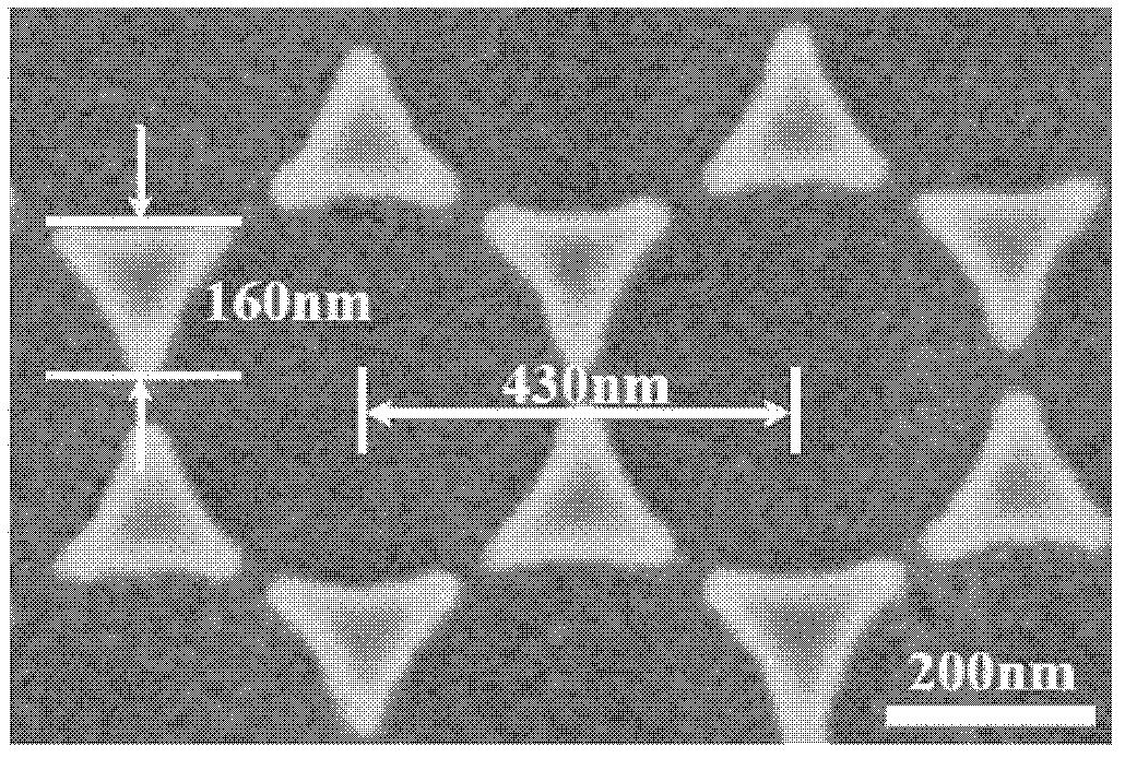
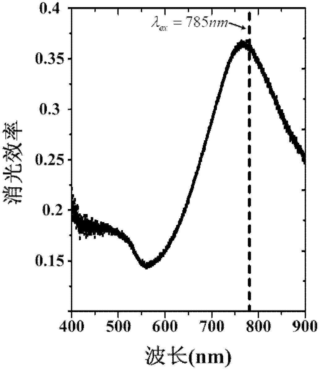
[0028] Example 1, using the present invention to realize the preparation and characterization of a surface-enhanced Raman chip with a structural period of 430nm and a particle diameter of 160nm with a localized surface plasmon resonance wavelength of 780nm.
[0029] (1) Choose quartz glass with a size of 1 cm × 1 cm double-sided fine polishing as the chip substrate, and after the substrate is cleaned and hydrophilized, take a monodisperse polystyrene nanosphere aqueous solution with a diameter of 430 nm and a concentration of 10%. Microliter drops onto the glass substrate for self-assembly, and after drying at room temperature, a single-layer array of polystyrene nanospheres is obtained;
[0030] (2) Etch the self-assembled polystyrene nanospheres with a reactive ion etching machine using oxygen, the power is 8W, the oxygen flow rate is 20SCCM, and the etching time is 165s;
[0031] (3) Put the etched polystyrene nanospheres into the working chamber of the vacuum coating syste...
Embodiment 2
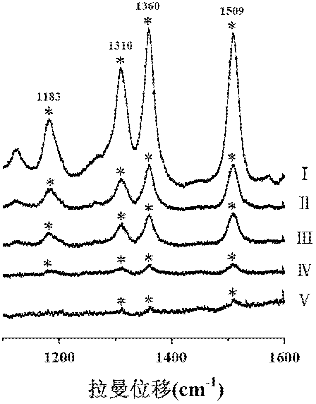
[0034] Example 2, using the present invention to realize the application of a surface-enhanced Raman chip with a structural period of 430nm, a particle diameter of 160nm, and a localized surface plasmon resonance wavelength of 780nm.
[0035] (1) Choose the quartz glass that size is 1cm * 1cm two-sided fine polishing as chip substrate, substrate is cleaned, hydrophilic treatment; Get diameter and be 430nm, concentration is the monodisperse polystyrene nanosphere aqueous solution 6 micrometers of 10%. Dropping onto a glass substrate for self-assembly, and drying at room temperature to obtain a single-layer array of polystyrene nanospheres;
[0036](2) Etching the self-assembled polystyrene nanospheres with a reactive ion etching machine using oxygen, the power is 5W, the oxygen flow rate is 20SCCM, and the etching time is 240s;
[0037] (3) Put the etched polystyrene nanospheres into the working chamber of the vacuum coating system at 2.8×10 -4 Deposit a layer of silver film o...
Embodiment 3
[0041] Example 3, using the present invention to test the stability of a surface-enhanced Raman chip with a structural period of 430nm and a particle diameter of 160nm with a localized surface plasmon resonance wavelength of 780nm.
[0042] (1) Choose the quartz glass that size is 1cm * 1cm two-sided fine polishing as chip substrate, substrate is cleaned, hydrophilic treatment; Get diameter and be 430nm, concentration is the monodisperse polystyrene nanosphere aqueous solution 6 micrometers of 10%. Dropping onto a glass substrate for self-assembly, and drying at room temperature to obtain a single-layer array of polystyrene nanospheres;
[0043] (2) Etching the self-assembled polystyrene nanospheres with a reactive ion etching machine using oxygen, the power is 6W, the oxygen flow rate is 20SCCM, and the etching time is 190s;
[0044] (3) Put the etched polystyrene nanospheres into the working chamber of the vacuum coating system at 2.6×10 -4 Deposit a layer of silver film on...
PUM
| Property | Measurement | Unit |
|---|---|---|
| Diameter | aaaaa | aaaaa |
| Diameter | aaaaa | aaaaa |
Abstract
Description
Claims
Application Information
 - R&D
- Intellectual Property
- Life Sciences
- Materials
- Tech Scout
- Unparalleled Data Quality
- Higher Quality Content
- 60% Fewer Hallucinations
Browse by: Latest US Patents, China's latest patents, Technical Efficacy Thesaurus, Application Domain, Technology Topic, Popular Technical Reports.
© 2025 PatSnap. All rights reserved.Legal|Privacy policy|Modern Slavery Act Transparency Statement|Sitemap|About US| Contact US: help@patsnap.com


