MOS (Metal Oxide Semiconductor) transistor and manufacturing method thereof
A technology of a MOS transistor and a manufacturing method, which is applied to the field of MOS transistors and their manufacturing, can solve the problems of limited electric field improvement, etc., and achieve the effects of increasing carrier mobility, increasing productivity, and increasing driving current.
- Summary
- Abstract
- Description
- Claims
- Application Information
AI Technical Summary
Problems solved by technology
Method used
Image
Examples
Embodiment 1
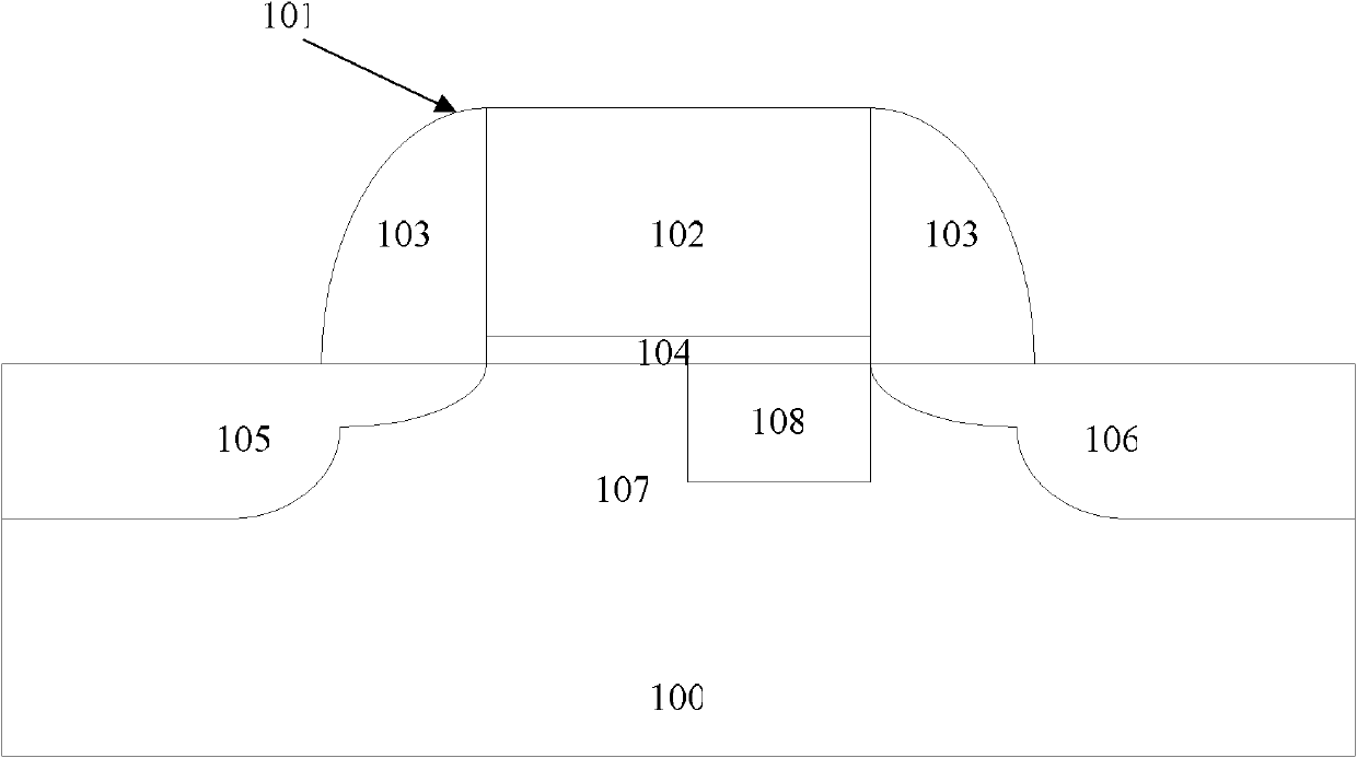
[0054] image 3 It is a schematic diagram of the structure of the PMOS transistor in this embodiment. As shown, the PMOS transistors include:
[0055] a semiconductor substrate 100;
[0056] a gate structure 101 on the semiconductor substrate 100;
[0057] a source region 105 and a drain region 106 in the surface of the semiconductor substrate 100 on both sides of the gate structure 101;
[0058] the channel 107 under the gate structure 101;
[0059] One end (drain end) of the channel 107 close to the drain region 106 has a heterogeneous region 108 , and the dielectric constant of the heterogeneous region 108 is greater than that of other regions in the channel 107 .
[0060] Among them, the semiconductor substrate 100 can be a bulk material composed of elemental semiconductors or components, such as silicon or silicon germanium with a single crystal, polycrystalline or amorphous structure, or a bulk material composed of compound semiconductors, such as silicon carbide, in...
Embodiment 2
[0079] Figure 5 It is a flow chart of the manufacturing method of the MOS transistor in the present embodiment, Figure 6 to Figure 12 It is a schematic diagram of the manufacturing method of the MOS transistor in this embodiment.
[0080] As shown in the figure, the manufacturing method of the MOS transistor includes:
[0081] Step S1: see Figure 6 , provide a semiconductor substrate 100, the semiconductor substrate 100 has a dummy gate structure 101', and a source region 105 and a drain region 106 in the surface of the semiconductor substrate on both sides of the dummy gate structure 101', wherein the source region Between 105 and the drain region 106 is a channel 107 , and the dummy gate structure includes: a dummy gate 102 ′, a dummy gate dielectric layer 104 ′, and gate spacers 103 on both sides of the dummy gate.
[0082] The structure on the semiconductor substrate 100 adopts the traditional manufacturing method of an asymmetric channel MOS transistor, and the dopi...
Embodiment 3
[0113] Figure 18 to Figure 19 It is a schematic diagram of the manufacturing method of the MOS transistor in the present embodiment, and the difference from the second embodiment is that a traditional photoresist process is used to form the pattern of the heterogeneous region.
[0114] like Figure 18 As shown, a photoresist layer 301 is formed on the surface of the substrate after removing the dummy gate, and the photoresist layer 301 covers both the inner and outer surfaces of the gate trench 310 .
[0115] like Figure 19 As shown, using a mask plate (MASK) with a heterogeneous region pattern for alignment and exposure, an opening 311 c is formed in the photoresist layer 301 , that is, the heterogeneous region pattern is transferred into the photoresist layer 301 . Afterwards, using the photoresist layer 301 as the heterogeneous region mask layer, etching the dummy gate dielectric layer and the channel part not covered by the heterogeneous region mask layer, forming a he...
PUM
| Property | Measurement | Unit |
|---|---|---|
| Thickness | aaaaa | aaaaa |
| Thickness | aaaaa | aaaaa |
Abstract
Description
Claims
Application Information
 - R&D Engineer
- R&D Manager
- IP Professional
- Industry Leading Data Capabilities
- Powerful AI technology
- Patent DNA Extraction
Browse by: Latest US Patents, China's latest patents, Technical Efficacy Thesaurus, Application Domain, Technology Topic, Popular Technical Reports.
© 2024 PatSnap. All rights reserved.Legal|Privacy policy|Modern Slavery Act Transparency Statement|Sitemap|About US| Contact US: help@patsnap.com


