Substrate structure with high mobility and preparation method thereof
A substrate structure, high mobility technology, applied in semiconductor/solid state device manufacturing, semiconductor devices, electrical components, etc., to reduce power consumption, achieve monolithic integration, broad application prospects and market prospects
- Summary
- Abstract
- Description
- Claims
- Application Information
AI Technical Summary
Problems solved by technology
Method used
Image


Examples
Embodiment Construction
[0033] In order to make the object, technical solution and advantages of the present invention clearer, the present invention will be described in further detail below in conjunction with specific embodiments and with reference to the accompanying drawings.
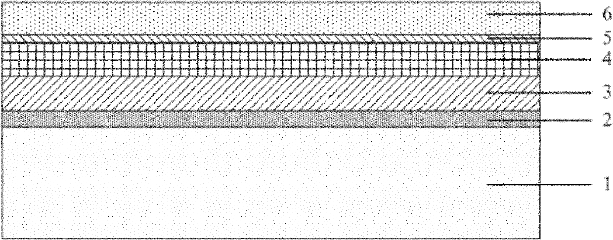
[0034] Such as figure 1 as shown, figure 1 It is a schematic diagram of the high mobility substrate structure provided by the present invention, and the high mobility substrate structure includes a single crystal silicon substrate 1, a buffer layer 2, a barrier layer 3, an indium gallium arsenide single crystal layer 4, a barrier layer 5 and germanium single crystal layer 6; the single crystal silicon substrate 1 is located at the bottom of the high mobility substrate structure; the buffer layer 2 is stacked on the single crystal silicon substrate 1; the potential The barrier layer 3 is stacked on the buffer layer 2; the InGaAs single crystal layer 4 is stacked on the barrier layer 3; the barrier layer 5 is stacked on th...
PUM
| Property | Measurement | Unit |
|---|---|---|
| Thickness | aaaaa | aaaaa |
| Thickness | aaaaa | aaaaa |
| Thickness | aaaaa | aaaaa |
Abstract
Description
Claims
Application Information
 - R&D
- Intellectual Property
- Life Sciences
- Materials
- Tech Scout
- Unparalleled Data Quality
- Higher Quality Content
- 60% Fewer Hallucinations
Browse by: Latest US Patents, China's latest patents, Technical Efficacy Thesaurus, Application Domain, Technology Topic, Popular Technical Reports.
© 2025 PatSnap. All rights reserved.Legal|Privacy policy|Modern Slavery Act Transparency Statement|Sitemap|About US| Contact US: help@patsnap.com