Manufacturing method of interconnection structure

A manufacturing method and hard mask layer technology, which are applied in semiconductor/solid-state device manufacturing, electrical components, circuits, etc., can solve the problems of decreased yield, increased difficulty of metal layers, failure of electrical connection of interconnect structures, etc. Small difficulty, the effect of avoiding the failure of electrical connection

Active Publication Date: 2014-09-03
SEMICONDUCTOR MANUFACTURING INTERNATIONAL (BEIJING) CORP
View PDF4 Cites 0 Cited by
  • Summary
  • Abstract
  • Description
  • Claims
  • Application Information

AI Technical Summary

Problems solved by technology

[0008] The concave surface will increase the difficulty of filling the metal layer in the subsequent method, and in severe cases, it will also cause the failure of the electrical connection of the interconnection structure, resulting in a decrease in yield

Method used


Image

  • Manufacturing method of interconnection structure
  • Manufacturing method of interconnection structure
  • Manufacturing method of interconnection structure

Examples


Embodiment Construction

[0028] In order to make the above objects, features and advantages of the present invention more comprehensible, specific implementations of the present invention will be described in detail below in conjunction with the accompanying drawings.

[0029] In the following description, many specific details are set forth in order to fully understand the present invention, but the present invention can also be implemented in other ways than those described here, so the present invention is not limited by the specific embodiments disclosed below.

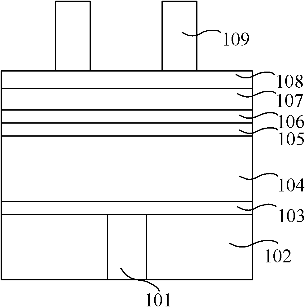
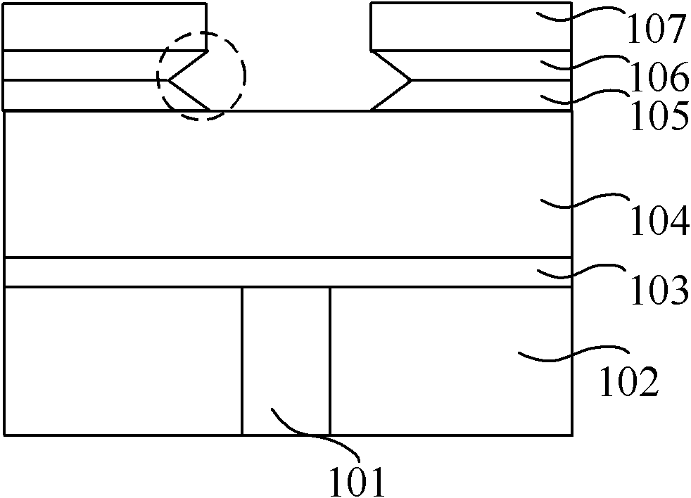
[0030] As described in the background, in the manufacturing method of the prior art interconnection structure, the hard mask layer is usually removed by wet cleaning method, and it is easy to form an oxide layer and a hard mask layer between the hard mask layer and the low-K dielectric layer. The concave surface surrounded by the low-K dielectric layer will increase the difficulty of filling the metal layer in the subsequent method.

[00...


PUM


Abstract

The invention discloses a manufacturing method of an interconnection structure. The method comprises the following steps of: providing a plug; forming a blocking layer, a low-K dielectric layer, a hard-mask low-K dielectric layer, an oxidation layer, a hard mask layer and a photoresist layer on the plug in sequence; patterning the photoresist layer and forming a photoresist pattern; etching the hard mask layer by using the photoresist pattern as a mask and forming an opening which is positioned in the hard mask layer and above the plug; removing the photoresist pattern, and etching the oxidation layer, the hard-mask low-K dielectric layer and the low-K dielectric layer exposed by the opening in sequence till the blocking layer is exposed; removing the hard mask layer, wherein a removing process has larger selection ratio for the hard mask layer than the oxidation layer and the hard-mask low-K dielectric layer; carrying out cleaning; and filling a conducting material into the opening. According to the manufacturing method of the interconnection structure provided by the invention, the yield can be improved.

Description

technical field [0001] The invention relates to the field of semiconductor manufacturing, in particular to a method for manufacturing an interconnection structure. Background technique [0002] With the continuous development of semiconductor manufacturing technology, the feature size is getting smaller and smaller, and the integration of integrated circuits is getting better and better. The integrated circuit is usually a structure with multiple semiconductor layers, and the semiconductor layers are interconnected by The structure realizes the electrical connection. A structure of an interconnection structure is disclosed in the Chinese patent application publication number CN101378047A. [0003] refer to figure 1 to reference figure 2 , shows a schematic side view of an interconnection structure formed by an embodiment of a method for manufacturing an interconnection structure in the prior art. [0004] Such as figure 1 As shown, the manufacturing method of the inter...

Claims


Application Information

Patent Timeline
Patent Type & Authority Patents(China)
IPC IPC(8): H01L21/768
Inventor 周鸣
Owner SEMICONDUCTOR MANUFACTURING INTERNATIONAL (BEIJING) CORP
Why Eureka
Try Eureka