


Quick Research
Generate reliable direction feasibility study reports for your R&D in just a few steps.

Technical Q&A
Discover and master advanced knowledge NOW. Basics, ideas, possibilities, all at once.

Find Solutions
As an expert in R&D theories, this can generate solutions to your technical problems instantly.

Evaluate Feasibility
Analyze your overall solution with one click, know your potential R&D risks in advance.

Monitor Landscape
Get weekly tech updates, stay abreast of the latest tech innovations and key insights.
Preparation method for epitaxial diode array isolated by double shallow trenches
A diode array and double shallow channel technology, which is applied in the field of epitaxial diode array preparation, can solve the problems of leakage current increase, inhomogeneity, increase of signals between adjacent word lines, etc., and achieve the effect of suppressing crosstalk current
- Summary
- Abstract
- Description
- Claims
- Application Information
AI Technical Summary
Problems solved by technology
Method used
Image

Examples
Embodiment 1
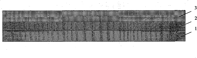
[0032] see Figure 1A-Figure 1H , this embodiment provides a method for preparing a double shallow trench isolation epitaxial diode array for phase-change memory, but the method for preparing a diode array of the present invention is not limited to application in phase-change memory, and can also be applied to other types of Storage devices, such as resistance memory, magnetic memory and ferroelectric memory etc., the method comprises the steps:
[0033] (1) On the substrate 1 of the first conductivity type (P type), a heavily doped first conductivity type (P+ type) region 2 and a highly doped second conductivity type region 2 are formed in the region where the diode array is located by ion implantation. Type (N++ type) area 3; as Figure 1A As shown, the main purpose of the heavily doped first conductivity type (P+ type) region 2 is to reduce the leakage between word lines, and the highly doped second conductivity type (N++ type) region 3 is used as a low resistance word lin...
Embodiment 2
[0042] By optimizing the preparation method, this embodiment provides a method for suppressing the crosstalk current between the bit lines of the double shallow trench isolation diode array:
[0043] (1) First, on the substrate of the first conductivity type (P type), form a heavily doped first conductivity type (P+ type) region and a highly doped second conductivity type region by ion implantation in the region where the diode array is located (N++ type) area; such as Figure 1A As shown; the main purpose of the heavily doped first conductivity type (P+ type) region is to reduce the leakage between word lines, and the highly doped second conductivity type (N++ type) region is used as a low resistance word line buried layer, in vacuum, after annealing, the depth of the word lines is greater than 0.2 microns, and the typical widths are 0.4 microns, 0.5 microns, 0.6 microns, 0.7 microns, etc.
[0044] (2) Deposit an intrinsic epitaxial layer on the highly doped second conductiv...
Embodiment 3
[0052] By optimizing the preparation method, this embodiment provides a method for suppressing the crosstalk current between the word lines of the double shallow trench isolation diode array:
[0053] (1) First, on the substrate of the first conductivity type (P type), form a heavily doped first conductivity type (P+ type) region and a highly doped second conductivity type region by ion implantation in the region where the diode array is located (N++ type) area ( Figure 1A ), the highly doped second conductivity type (N++ type) region is used as a low-resistance word line buried layer. After rapid annealing in vacuum, the width of the word line is greater than 0.2 microns, and the typical width is 0.4 microns, 0.5 microns , 0.6 microns, 0.7 microns, etc.
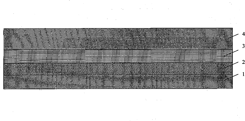
[0054] (2) Deposit an intrinsic epitaxial layer on the buried layer by chemical vapor phase epitaxy, with a typical thickness of 0.2-0.8 microns, such as Figure 1B shown.
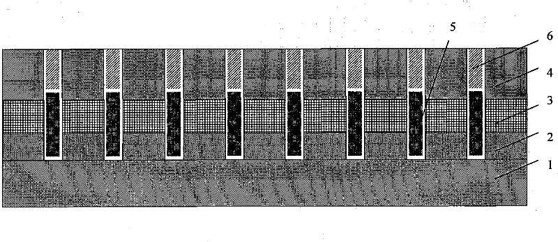
[0055] (3) Deep trenches are formed by photoli...
PUM
 Abstract
Description
Claims
Application Information
 - R&D Engineer
- R&D Manager
- IP Professional
- Industry Leading Data Capabilities
- Powerful AI technology
- Patent DNA Extraction
Browse by: Latest US Patents, China's latest patents, Technical Efficacy Thesaurus, Application Domain, Technology Topic, Popular Technical Reports.
© 2024 PatSnap. All rights reserved.Legal|Privacy policy|Modern Slavery Act Transparency Statement|Sitemap|About US| Contact US: help@patsnap.com