Semiconductor device and semiconductor integrated circuit using the same
a technology of semiconductor integrated circuit and semiconductor, which is applied in the direction of semiconductor devices, semiconductor/solid-state device details, electrical apparatus, etc., can solve the problems of increasing leakage current, difficult to suppress leakage current to a target value, and increasing leakage current from mos transistors, so as to improve the driving capability of mos transistors and high processing performance. , the effect of high processing performan
- Summary
- Abstract
- Description
- Claims
- Application Information
AI Technical Summary
Benefits of technology
Problems solved by technology
Method used
Image
Examples
first embodiment
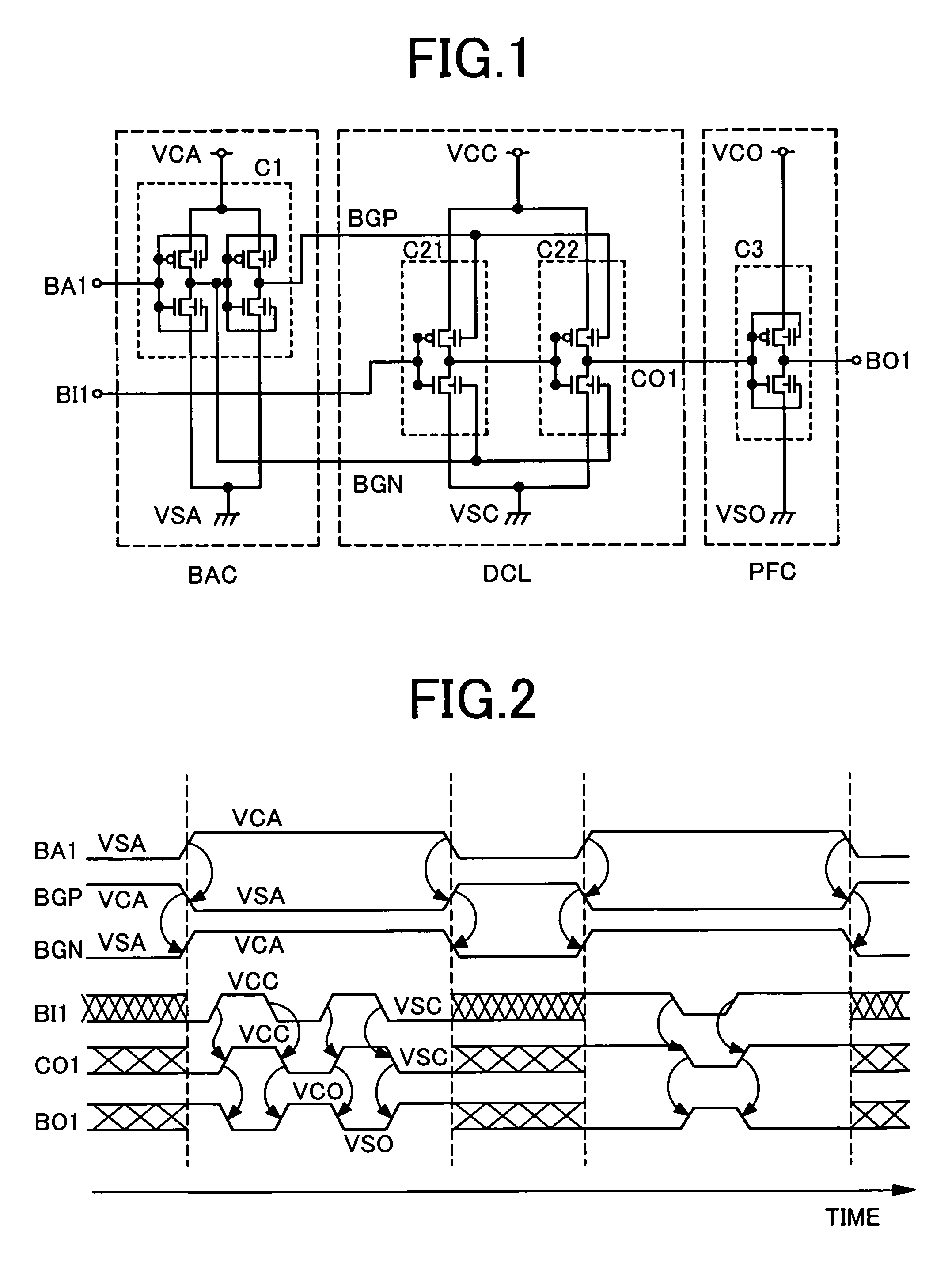
[0057]FIG. 1 illustrates a first embodiment of the present invention.
[0058]The circuit shown in FIG. 1 is largely classified to three blocks. A block DCL is a logic circuit block, a BAC block is a circuit for controlling a back gate of the Block DCL, and a PFC block is a circuit for driving an output terminal BO1 generally having a heavy load.
[0059]The DCL block is an example of a logic circuit with inverter circuits in two stages. Sign BI1 denotes an input to the DCL block and CO1 denotes an output from the DCL block. Sign VCC denotes a power voltage and sign VSC denotes the ground voltage. The signs C21 and C22 denote inverter circuits respectively, and BI1 denotes the input to the inverter circuit C21. An output from the inverter circuit C21 is provided as an input to the inverter circuit 22, and CO1 denotes an output terminal of the inverter circuit C22. In this logic circuit block DCL, namely in the two stages of inverter circuits in FIG. 1, a CMOS transistor constituting the l...
second embodiment
[0078]The DCL shown in FIG. 1 is a logic circuit block as described above, and is activated by the circuit BAC and executes computing operations. Another example is shown in FIG. 7.
[0079]The DCL shown in FIG. 7 includes a NAND circuit C2 and a NOR circuit C3. In both of the circuits, back gates of each pMOS transistor are generically denoted by sign BGP, and back gates of each nMOS transistor are generically denoted by sign BGN. Generally, an input terminal for inputting a signal from outside the DCL is only the input terminal BI1. However, there may be another terminal for inputting a signal from outside the DCL. Although a terminal C2N1 and a terminal C3N1 is not shown in the figure, the terminals are connected to output terminals of other circuit in the DCL, and received signals outputted from the terminals. The block PFC includes inverters provided in two stages. Like the case shown in FIG. 1, in the blocks BAC and PFC, the gates and the back gates are connected directly.
[0080]F...
third embodiment
[0081]FIG. 9 illustrates an example of another logic circuit used in the DCL. Signs pc, carry, s, s1, and SUM denote an input / output signal. Back gates of the pMOS transistor are connected to the BGP terminal. Back gates of each nMOS transistor are connected to the BGN terminal. In this embodiment, circuits GK are provided at some nodes in the block. The circuits GK are latch circuits for retaining signals. The latch circuit is used to stabilize a signal level at nodes connected during the standby state. In the activated state, a drive current should be weak so that a current actually driving the nodes will not be impeded.
PUM
 Abstract
Description
Claims
Application Information
 - R&D
- Intellectual Property
- Life Sciences
- Materials
- Tech Scout
- Unparalleled Data Quality
- Higher Quality Content
- 60% Fewer Hallucinations
Browse by: Latest US Patents, China's latest patents, Technical Efficacy Thesaurus, Application Domain, Technology Topic, Popular Technical Reports.
© 2025 PatSnap. All rights reserved.Legal|Privacy policy|Modern Slavery Act Transparency Statement|Sitemap|About US| Contact US: help@patsnap.com


