Method for manufacturing split gate flash by reducing writing interference

A fabrication method and separation gate technology, applied in semiconductor/solid-state device manufacturing, electrical components, circuits, etc., can solve problems such as easy generation of tunneling current, separation gate flash memory write interference, etc., to avoid write interference, reduce Tunneling current, effect of preventing write variation

Active Publication Date: 2012-03-14
SEMICONDUCTOR MANUFACTURING INTERNATIONAL (BEIJING) CORP +1
View PDF3 Cites 5 Cited by
  • Summary
  • Abstract
  • Description
  • Claims
  • Application Information

AI Technical Summary

Problems solved by technology

However, as shown in FIG. 1 , this step will cause the concentration difference between the concentration in the substrate region 100 below the gap between the word line 113' and the floating gate 105' and the concentration in the channel 104' below the word line 113' to be too large. , when the PN junction formed at the junction of the channel 104' and the semiconductor substrate 100' is reverse biased, it is easy to generate a tunneling current, and the tunneling current enters the floating gate 105' under the action of the voltage of the control gate 109', Write changes are made to cells that should not be changed. Therefore, the manufacturing method of split gate flash memory in the prior art is likely to cause write disturbance

Method used


Image

  • Method for manufacturing split gate flash by reducing writing interference
  • Method for manufacturing split gate flash by reducing writing interference
  • Method for manufacturing split gate flash by reducing writing interference

Examples


Embodiment Construction

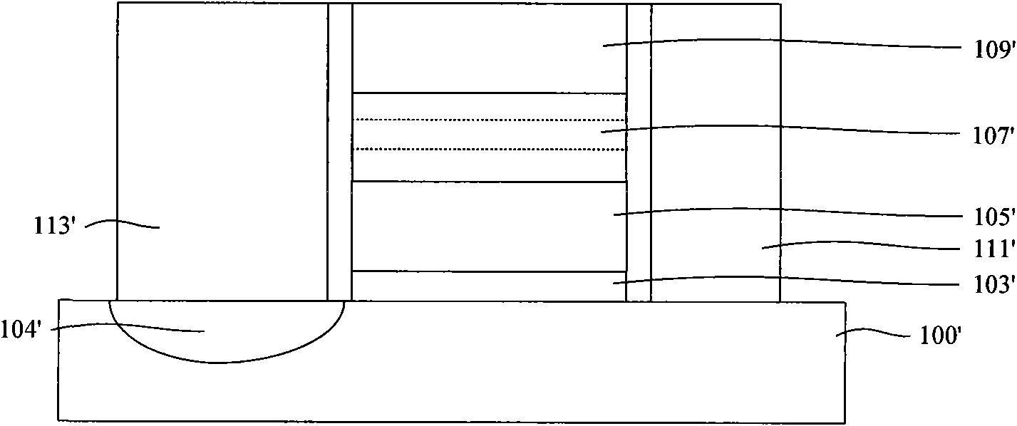
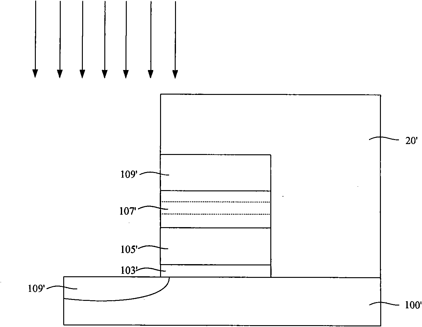
[0031] In order to make the content of the present invention clearer and easier to understand, the content of the present invention will be further described below in conjunction with the accompanying drawings.

[0032] In the following description, specific details are set forth in order to provide a thorough understanding of the present invention. Of course, the present invention is not limited to this specific embodiment, and general replacements known to those skilled in the art are also covered within the protection scope of the present invention. Accordingly, the present invention is not limited to the specific examples disclosed below.

[0033] Next, the above and other objects, features and advantages of the present invention will be more apparent through a more specific description of preferred embodiments of the present invention shown in the accompanying drawings. Like reference numerals designate like parts throughout the drawings. The drawings are not intended t...


PUM


Abstract

The invention discloses a method for manufacturing a split gate flash by reducing writing interference. After a control gate, a floating gate, an erasing gate and a word line are formed on a semiconductor substrate, lightly-doped ions are implanted; and the iron implantation comprises a vertically lightly doping step and a pocket ion implantation step, wherein in the pocket ion implantation step, an ion beam is injected into the semiconductor substrate below the word line at an inclined angle. By the method for manufacturing the split gate flash, an ion implantation step which is used for defining threshold value voltage of a flash unit in the prior art is eliminated; after a step of forming the word line, the pocket ion implantation step is added to reduce the doping concentration of a substrate area below a clearance between the word line and the floating gate, so that the difference of the doping concentration of the substrate area below the clearance between the word line and the floating gate and the doping concentration between the concentrations of channels below the floating gate is reduced; therefore, a writing unit which is not ought to have a writing change is prevented from having the writing change, and the writing interference is effectively avoided.

Description

technical field [0001] The invention relates to the field of semiconductor technology, in particular to a method for manufacturing a split-gate flash memory that reduces write disturbance. Background technique [0002] In the current semiconductor industry, collective circuit products can be mainly divided into three types: logic, memory and analog circuits, among which memory devices account for a considerable proportion of integrated circuit products. Memory is used to store a large amount of digital information. According to recent surveys, memory chips account for about 30% of semiconductor transactions worldwide. Over the years, technological progress and market demand have led to more and more high-density various Types of memory, such as RAM (random access memory), DRAM (dynamic random access memory), ROM (read-only memory), EPROM (erasable memory programmable memory), FLASH (flash memory) and FRAM (ferroelectric memory), etc. Among the memories, the development of t...

Claims


Application Information

Patent Timeline
Patent Type & Authority Applications(China)
IPC IPC(8): H01L21/8247
Inventor 周儒领李勇
Owner SEMICONDUCTOR MANUFACTURING INTERNATIONAL (BEIJING) CORP
Why Eureka
Try Eureka