Insulated gate bipolar transistor (IGBT) with anti-latchup effect

A bipolar transistor and insulated gate technology, applied in semiconductor devices, electrical components, circuits, etc., can solve the problems of reducing the resistivity of the P-type base region, increasing the forward voltage drop of the device, and reducing the conductance modulation effect in the drift region. , to achieve the effect of improving current carrying capacity, avoiding latch-up effect, and large safe working area

Inactive Publication Date: 2012-02-15
UNIV OF ELECTRONIC SCI & TECH OF CHINA +1
View PDF2 Cites 6 Cited by
  • Summary
  • Abstract
  • Description
  • Claims
  • Application Information

AI Technical Summary

Problems solved by technology

However this leads to N - The conductance modulation effect in the drift region is reduced, which increases the forward voltage drop of the device, which is undesirable
2) Reduce the resistivity of the P-type base region
The resistance of the P-type base region under the N-type source region is proportional to the length of the N-type source region. By reducing the length of the N-type source region, the resistance of the P-type base region can be reduced, but this is limited by the process conditions.

Method used


Image

  • Insulated gate bipolar transistor (IGBT) with anti-latchup effect
  • Insulated gate bipolar transistor (IGBT) with anti-latchup effect
  • Insulated gate bipolar transistor (IGBT) with anti-latchup effect

Examples


Embodiment Construction

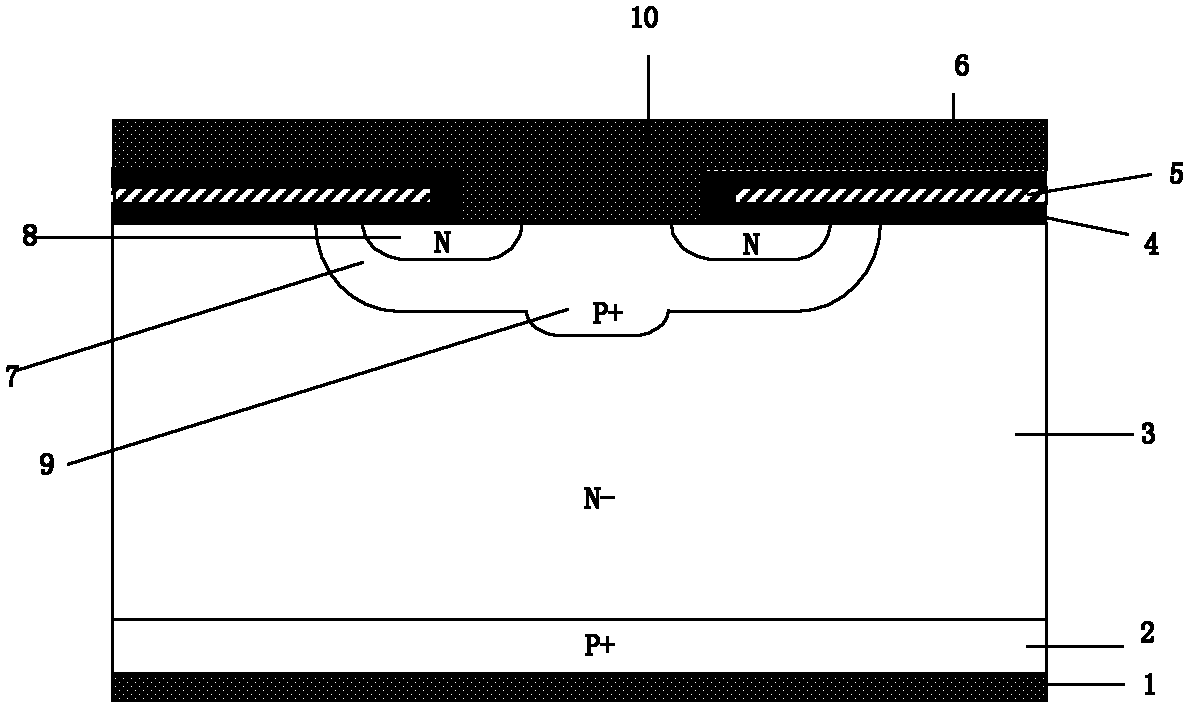
[0019] A latch-up resistant insulated gate bipolar transistor, such as figure 2 As shown, in the P-type base region 7 and N - A dielectric isolation layer 11 is provided at the interface between the drift regions 3 .

[0020] In the above scheme:

[0021] The material of the isolation dielectric layer 11 can be SiO 2 .

[0022] The isolation dielectric layer 11SiO 2 It can be formed by oxygen ion implantation and annealing. Select an N-type substrate FZ silicon wafer with a suitable resistivity crystal orientation according to the required withstand voltage, implant oxygen ions in a specific area, anneal to form the required dielectric layer, grow field oxygen, make the terminal part, and engrave the active area Etching and long gate oxide, depositing polysilicon gate, etching polysilicon gate, implanting P-type base region and annealing, implanting N-type source region and annealing, thick oxide layer, etching contact hole, implanting P+ body region, depositing front m...


PUM


Abstract

The invention discloses an insulated gate bipolar transistor (IGBT) with an anti-latchup effect, belonging to the technical field of power semiconductor devices. In the invention, partial SOI silicon wafer is used through an ion implantation, deposition or thermal growth method or directly; an isolation medium layer is arranged on the interface between the P-type base region and an N-drift region; a current channel for the hole current in the N-drift region to flow into an N-type source region through the P-type base region is blocked; and therefore, the opening of a parasitic NPN transistor in the IGBT structure can be effectively prevented, and the latchup effect caused by the NPNP structure in the IGBT is avoided so as to improve the current bearing capability of the device and providing a larger safe working region. The IGBT provided by the invention can be applied to the field of low-power and high-power semiconductor power devices as well as power integration circuits.

Description

technical field [0001] The invention belongs to the technical field of power semiconductor devices, and relates to insulated gate bipolar transistors (IGBTs), more specifically, to IGBT devices resistant to latch-up effects. Background technique [0002] As an indispensable core device of contemporary power electronics technology, power devices have developed rapidly in recent decades. With the continuous deepening of research, power devices have been developing in the direction of high frequency, high withstand voltage and low loss. As a gate-controlled switching device, IGBT uses the conductance modulation effect to reduce the conductance voltage drop of the device, caters to the development direction of power devices, and becomes an indispensable power product for medium and high voltage switches and intermediate frequency inverters. [0003] The traditional IGBT device structure such as figure 1 As shown, N-type source region 8, P-type base region 7, N - Drift Zone 3 ...

Claims


Application Information

Patent Timeline
IPC IPC(8): H01L29/739H01L29/10
Inventor 李泽宏杨文韬张金平张波
Owner UNIV OF ELECTRONIC SCI & TECH OF CHINA
Why Eureka
Try Eureka