Anti-latch circuit and integrated circuit

A latching circuit, power supply voltage technology, applied in circuits, electrical components, electronic switches, etc., can solve problems such as burnout and circuit failure to work properly, and achieve the effect of preventing latchup effect

Pending Publication Date: 2018-07-10
CHIPONE TECH BEIJINGCO LTD
View PDF0 Cites 2 Cited by
  • Summary
  • Abstract
  • Description
  • Claims
  • Application Information

AI Technical Summary

Problems solved by technology

There are parasitic transistors (also known as parasitic thyristors, SCR for short) in general integrated circuits. The latch-up effect means that the parasitic bipolar transistors are triggered and turned on, forming a low-impedance and large-current path between the power supply VDD and the ground GND. , causing the circuit to fail to work properly, or even burn out

Method used


Image

  • Anti-latch circuit and integrated circuit
  • Anti-latch circuit and integrated circuit
  • Anti-latch circuit and integrated circuit

Examples


Embodiment Construction

[0023] Various embodiments of the invention will be described in more detail below with reference to the accompanying drawings. In the various drawings, the same elements are denoted by the same or similar reference numerals. For the sake of clarity, various parts in the drawings have not been drawn to scale.

[0024] The specific implementation manners of the present invention will be further described in detail below in conjunction with the accompanying drawings and embodiments.

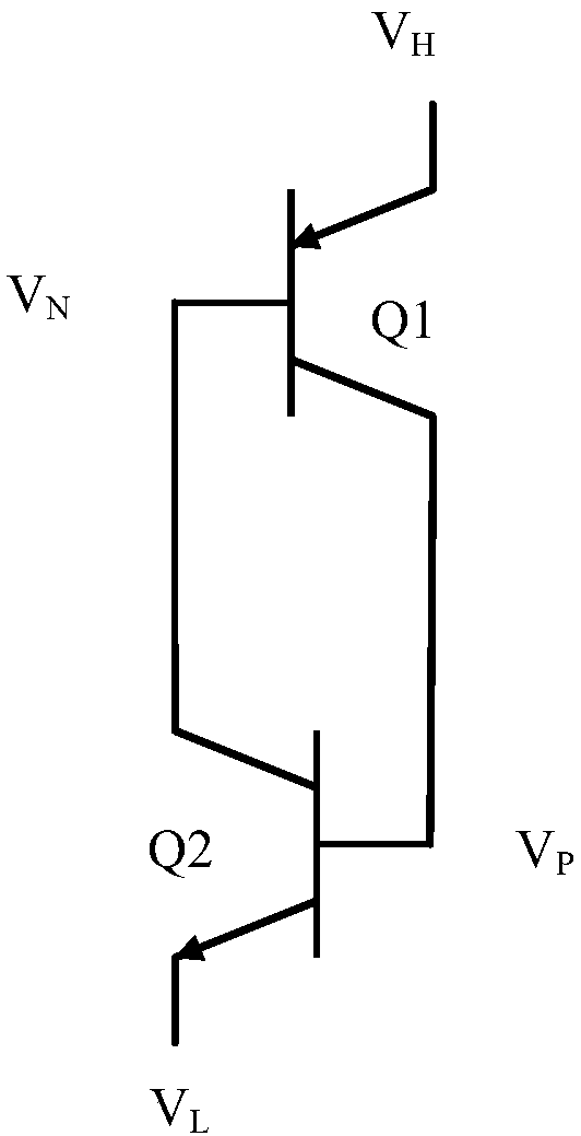
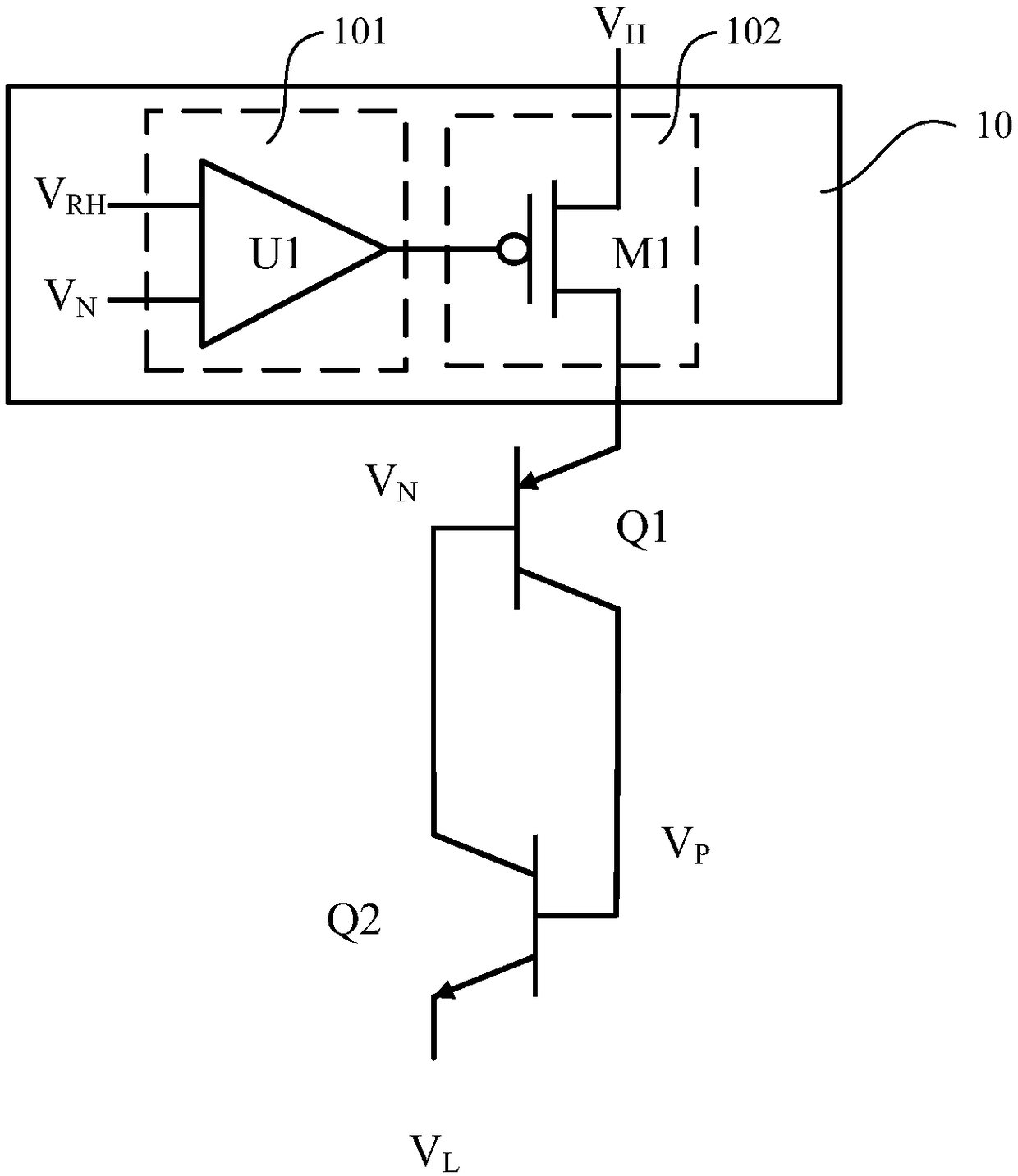
[0025] image 3 A circuit diagram of the anti-latch circuit provided by the first embodiment of the present invention is shown. Such as figure 1 As shown, the anti-latch circuit includes a first transistor Q1 and a second transistor Q2 and a control circuit 10 .

[0026] The first transistor Q1 has a control terminal, a first terminal and a second terminal, and the control terminal receives the first control voltage V N , the first terminal receives the first supply voltage V H .

[0027] Th...


PUM


Abstract

The invention discloses an anti-latch circuit, comprising a first transistor, a second transistor and a control circuit, wherein the control end of the first transistor receives a first control voltage, and a first end of the first transistor receives a first power supply voltage; the second transistor has an opposite type of the first transistor, the control end of the second transistor receivesa second control voltage and is connected with a second end of the first transistor, a first end of the second transistor is connected with the control end of the first transistor, and a second end ofthe second transistor receives a second power supply voltage; and the control circuit is arranged on a path formed by the first transistor and the second transistor between the first power supply voltage and the second power supply voltage and is used to cut off the path when the first control voltage and / or the second control voltage exceed / exceeds a preset range. According to the anti-latch circuit provided by the invention, the control circuit is arranged on the path formed by the first transistor and the second transistor between the first power supply voltage and the second power supplyvoltage, the control circuit cuts off the path when the first control voltage and / or the second control voltage exceed / exceeds the preset range, and thus the occurrence of a latch-up effect in a power-on state can be prevented.

Description

technical field [0001] The invention relates to the technical field of integrated circuits, in particular to an anti-latch circuit and an integrated circuit. Background technique [0002] With the development of the IC manufacturing process, the size of the chip is getting smaller and smaller, and the chip packaging density and integration are getting higher and higher, and the possibility of latch-up (Latch up) will increase, and the modules will interfere with each other. The possibility will also increase. There are parasitic transistors (also known as parasitic thyristors, SCR for short) in general integrated circuits. The latch-up effect means that the parasitic bipolar transistors are triggered and turned on, forming a low-impedance and large-current path between the power supply VDD and the ground GND. , causing the circuit to fail to work properly, or even burn out. Such parasitic bipolar transistors are found in various parts of integrated circuits, including inpu...

Claims


Application Information

Patent Timeline
IPC IPC(8): H03K17/081H03K17/687
CPCH03K17/08104H03K17/687H03K17/20H03K17/0826H03K17/60H03K17/081H03K17/6872H01L27/0262
Inventor 陈天豪吴俊杰
Owner CHIPONE TECH BEIJINGCO LTD
Why Eureka
Try Eureka