Static random access memory and method for manufacturing the same

A static random access and memory technology, which is applied in semiconductor/solid-state device manufacturing, electric solid-state devices, semiconductor devices, etc., and can solve the problems of increasing the integration of memory cells and low running speed of all CMOS SRAMs

Inactive Publication Date: 2007-07-04
DONGBU ELECTRONICS CO LTD
View PDF0 Cites 4 Cited by
  • Summary
  • Abstract
  • Description
  • Claims
  • Application Information

AI Technical Summary

Problems solved by technology

Also, the full CMOS type SRAM uses p-channel TFTs to increase the integration of memory cells due to its larger area
However, due to the high resistance of the power supply potential layer Vcc, the full CMOS type SRAM operates at a lower speed

Method used


Image

  • Static random access memory and method for manufacturing the same
  • Static random access memory and method for manufacturing the same
  • Static random access memory and method for manufacturing the same

Examples


Embodiment Construction

[0012] Hereinafter, a static random access memory (SRAM) and a method of manufacturing the memory according to an embodiment of the present invention will be described with reference to the accompanying drawings.

[0013] In the following description of the embodiments of the present invention, when one layer is formed on another layer, it may be directly formed on the other layer, or one or more intervening layers may appear.

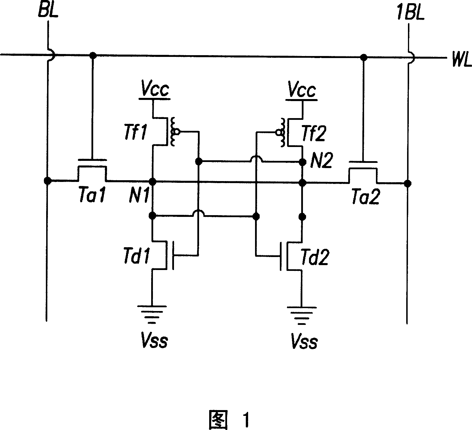
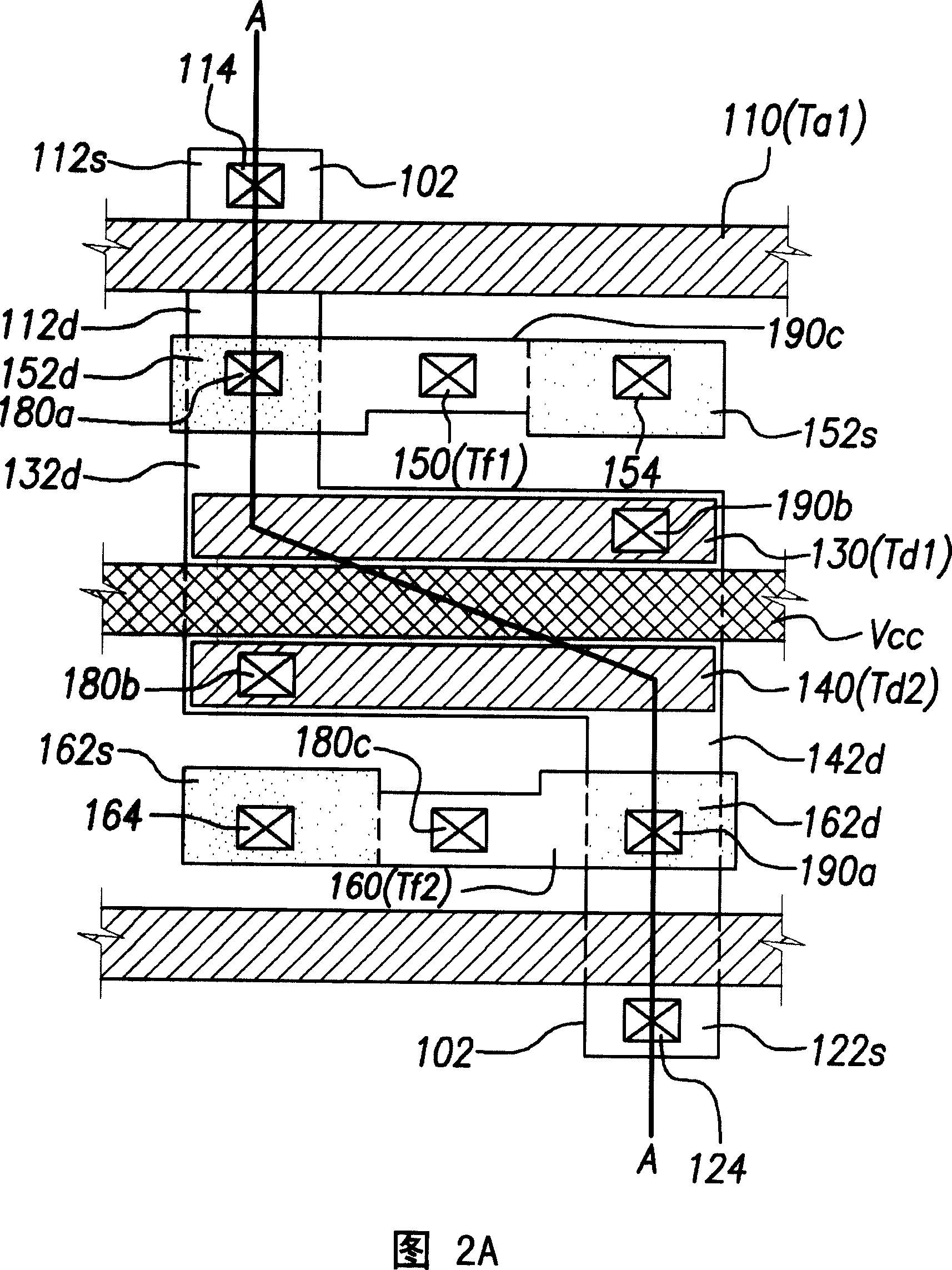
[0014] FIG. 1 is a circuit diagram showing a static random access memory (SRAM) according to an embodiment of the present invention. Here, the PMOS transistor is used as an example of a resistance device. And FIG. 2A is a layout diagram showing an SRAM according to an embodiment of the present invention, and FIG. 2B is a cross-sectional view taken along the line A-A of FIG. 2A.

[0015] 1, the SRAM cell includes: a first access NMOS transistor (TFT) Ta1 and a second access NMOS transistor (TFT) Ta2, the transistors are connected to the bit line through the...


PUM


Abstract

Disclosed is a static random access memory (SRAM), which includes first and second access transistors composed of metal oxide semiconductor (MOS) transistors, first and second drive transistors composed of MOS transistors, and first and second p-channel thin film transistors (TFTs) used as pull-up devices. The SRAM includes a ground potential layer disposed as a common source of the first and second drive transistors, and formed by implanting a dopant into a semiconductor substrate, a power supply potential layer connected with sources of the first and second p-channel TFTs, and an insulating layer formed on the substrate and interposed between the ground potential layer and the power supply potential layer.

Description

Technical field [0001] The present invention relates to a static random access memory (Random Access Memory, hereinafter referred to as SRAM) and a method for manufacturing the memory. Background technique [0002] Static random access memory (SRAM) is a storage device that can store data in a circuit using a latch manner. The SRAM device has high operating speed and low power consumption, and is different from dynamic random access memory (DRAM) in that it does not need to update the stored information regularly. [0003] Generally, SRAM includes two pull-down devices, two access devices, and two pull-up devices. The SRAM is divided into three types according to the structure of pull-down devices: fully complementary Complementary Metal-Oxide Semiconductor (CMOS) type, high load resistor (HLR) type, and thin film transistor (TFT) type. The full CMOS type SRAM uses a p-channel bulk metal oxide semiconductor field effect transistor (MOSFET) as a pull-down device. The HLR type SRAM...

Claims


Application Information

Patent Timeline
Patent Type & Authority Applications(China)
IPC IPC(8): H01L27/11H01L21/8244
CPCH01L27/1108H01L27/11Y10S257/903H10B10/125H10B10/00H10B99/00
Inventor 朴盛羲
Owner DONGBU ELECTRONICS CO LTD
Why Eureka
Try Eureka