Semiconductor device producing method
A manufacturing method and semiconductor technology, which are applied in semiconductor/solid-state device manufacturing, electrical components, circuits, etc., to achieve the effect of expanding the photolithography process window and eliminating coupling capacitance
- Summary
- Abstract
- Description
- Claims
- Application Information
AI Technical Summary
Problems solved by technology
Method used
Image

Examples
Embodiment 1
[0043] Combine below Figure 3A-3F The manufacturing process of the single damascene metal interconnection structure is introduced in detail. The redundant metal grooves formed in this embodiment have the same depth as the auxiliary pattern redundant metal grooves.
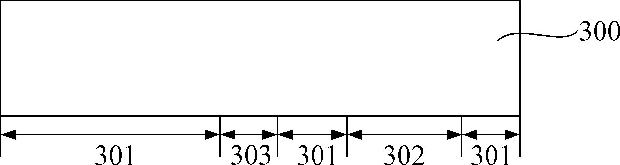
[0044] Such as Figure 3A As shown, first, a semiconductor substrate 300 is provided, and the semiconductor substrate 300 includes a redundant metal region 302, an auxiliary pattern redundant metal region 303 and a non-redundant metal region 301, that is, in addition to the redundant metal region 302 and the auxiliary pattern The region of the semiconductor substrate outside the redundant metal region 303 is the non-redundant metal region 301 . Wherein, the metal wiring is formed in the semiconductor substrate 300, since the present invention mainly relates to the manufacturing process of the metal damascene structure, so the process of forming the metal wiring in the semiconductor substrate 300 will not be intro...
Embodiment 2
[0053] This embodiment combines Figures 4A-4G The manufacturing process of the double damascene metal interconnection structure with the via hole etched first is introduced in detail, wherein the redundant metal groove and the auxiliary pattern redundant metal groove have the same depth (height).
[0054] Such as Figure 4A As shown, first, a semiconductor substrate 400 is provided, and the semiconductor substrate 400 includes a redundant metal region 402, an auxiliary pattern redundant metal region 403 and a non-redundant metal region 401, wherein except for the redundant metal region 402 and the auxiliary pattern redundant The region of the semiconductor substrate outside the redundant metal region 403 is the non-redundant metal region 401 .
[0055] Such as Figure 4B As shown, next, a dielectric layer 410 is formed on the semiconductor substrate 400 .
[0056] Such as Figure 4C As shown, next, the dielectric layer on the non-redundant metal region 401 is thinned.
...
Embodiment 3
[0063] This embodiment combines Figures 5A-5I The fabrication process of the self-aligned hard mask double damascene metal interconnection structure is introduced in detail, wherein the redundant metal groove and the auxiliary pattern redundant metal groove have the same depth (height).
[0064] Such as Figure 5A As shown, firstly, a semiconductor substrate 500 is provided, and the semiconductor substrate 500 includes a redundant metal region 502 , an auxiliary pattern redundant metal region 503 and a non-redundant metal region 501 .
[0065] Such as Figure 5B As shown, a dielectric layer 510 is formed on the semiconductor substrate 500 .
[0066] Such as Figure 5C As shown, the dielectric layer on the non-redundant metal region 501 is thinned.
[0067] Such as Figure 5D As shown, a self-aligned hard mask layer 530 is formed on the dielectric layer 510 .
[0068] Such as Figure 5E As shown, the self-aligned hard mask layer 530 is etched to form a hard mask metal w...
PUM
 Abstract
Description
Claims
Application Information
 - Generate Ideas
- Intellectual Property
- Life Sciences
- Materials
- Tech Scout
- Unparalleled Data Quality
- Higher Quality Content
- 60% Fewer Hallucinations
Browse by: Latest US Patents, China's latest patents, Technical Efficacy Thesaurus, Application Domain, Technology Topic, Popular Technical Reports.
© 2025 PatSnap. All rights reserved.Legal|Privacy policy|Modern Slavery Act Transparency Statement|Sitemap|About US| Contact US: help@patsnap.com