MSM (Metal-Semiconductor-Metal) photodetector with improved structure and preparation method thereof

A photodetector and improved structure technology, applied in the field of photodetection, can solve problems such as electron leakage, limited detection efficiency, and high requirements

Inactive Publication Date: 2012-01-18
SUZHOU INST OF NANO TECH & NANO BIONICS CHINESE ACEDEMY OF SCI
View PDF4 Cites 17 Cited by
  • Summary
  • Abstract
  • Description
  • Claims
  • Application Information

AI Technical Summary

Problems solved by technology

[0003] The traditional MSM structure detector directly adopts the steps of photolithography-depositing metal-stripping to obtain the surface electrode pattern on the surface of the material. This method is simple in process and easy to obtain a good Schottky contact. However, because the MSM structure belongs to the surface device structure, Therefore, the requirements on the surface of the material itself are relatively high. If there are a large number of defects and impurities on the surface of the material, a certain number of surface energy levels will be generated, and electron leakage channels will be formed under the action of an external bias voltage, and the dark current of the device will increase.
At the same time, since the MSM photodetector only utilizes part of the surface of the device material (the thickness of the active region is related to the attenuation depth of light in the absorbing material), its detection efficiency is limited

Method used


Image

  • MSM (Metal-Semiconductor-Metal) photodetector with improved structure and preparation method thereof
  • MSM (Metal-Semiconductor-Metal) photodetector with improved structure and preparation method thereof
  • MSM (Metal-Semiconductor-Metal) photodetector with improved structure and preparation method thereof

Examples


Embodiment Construction

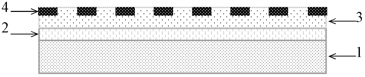
[0029] refer to figure 1 , The MSM detector of the buried electrode structure of the present invention includes a sapphire sink 1 , an AlN buffer layer 2 , a GaN active layer 3 , and a metal interdigitated electrode 4 from bottom to top. Its structural features are: the electrode structure buried in the material is used to replace the original surface electrode structure. In this way, the adverse effects of the surface state of the material on device performance such as increased dark current and poor metal contact performance can be improved. .

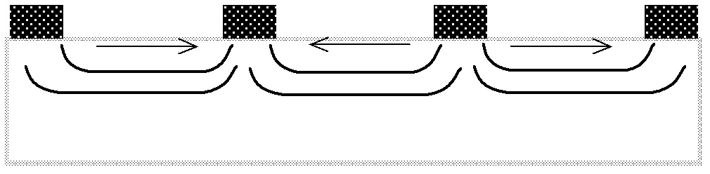
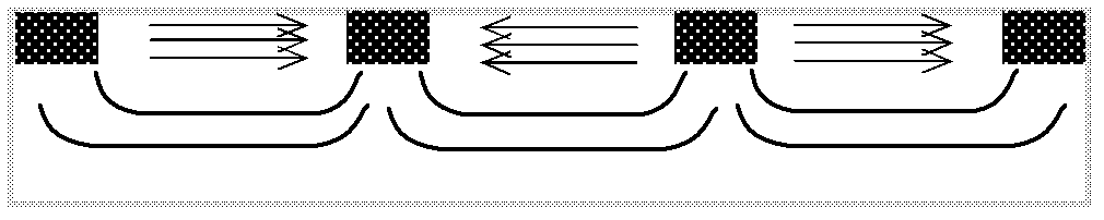
[0030] The electric field physical model of the MSM detector is as follows Figure 2a and Figure 2b shown, where Figure 2a It is a traditional planar electrode structure. For non-buried electrodes, the field strength decreases with the increase of the longitudinal depth of the active region. The attenuation is faster under the electrode and slower in the middle of the electrode. Figure 2b It is the buried electrode structure i...


PUM


Abstract

The invention discloses an MSM (Metal-Semiconductor-Metal) photodetector with an improved structure and a preparation method thereof. The detector comprises an active layer, a buffering layer and an insulating substrate arranged from upside to downside in sequence, wherein an electrode is also arranged on the active layer; and the electrode is at least locally buried in the active layer; the preparation method comprises the following steps of: etching an active layer surface mask overlapped on the insulating substrate to form a buried electrode channel and filling a conductive material in the buried electrode channel to form an electrode with a set form. According to the invention, the original surface electrode structure is replaced by the electrode structure buried in the semiconductor material so that the buried electrode can form an electric field in the horizontal direction in the interior of the material so as to obtain an electric field intensity stronger than that of a surface electrode structure; and the electron moves along an approximate straight track under the stronger field intensity effect so that the photon-generated carrier drift is accelerated, the response time of the device is effectively reduced, the responsiveness of the device is improved and the preparation process is simple and controllable.

Description

technical field [0001] The invention relates to a metal-semiconductor-metal (MSM) photodetector in the field of photodetection, in particular to an MSM photodetector with a buried interdigital structure and a preparation method thereof. Background technique [0002] Metal-semiconductor-metal (MSM) photodetectors use the Schottky barrier between the metal and semiconductor interfaces to form a carrier depletion region similar to a PN junction. The photogenerated carriers generated by the incident light in the semiconductor drift in the reverse Schottky junction depletion region under the action of an external electric field, and are quickly collected by the electrodes at both ends of the detector. This structure is equivalent to two back-to-back coplanar Schottky barrier connections. The metal contact is usually made in the shape of cross stripes directly on the semiconductor surface. Light can be absorbed in the electrode gap of the metal finger. The light detection of the M...

Claims


Application Information

Patent Timeline
Patent Type & Authority Applications(China)
IPC IPC(8): H01L31/11H01L31/0224H01L31/18
CPCY02P70/50
Inventor 李海军杨乐臣付凯刘冬熊敏张宝顺
Owner SUZHOU INST OF NANO TECH & NANO BIONICS CHINESE ACEDEMY OF SCI
Why Eureka
Try Eureka