Copper indium gallium selenium (CIGS) solar battery with gradient energy band and preparation method thereof
A solar cell, copper indium gallium selenide technology, applied in circuits, photovoltaic power generation, electrical components, etc., can solve the problems of battery photoelectric conversion efficiency reaching the limit, environmental damage, high energy consumption, etc., achieve good market promotion prospects, and improve absorption capacity , Improve the effect of conversion efficiency
- Summary
- Abstract
- Description
- Claims
- Application Information
AI Technical Summary
Problems solved by technology
Method used
Image
Examples
Embodiment 1
[0039] The sample preparation process uses the following steps:
[0040] (1) After ultrasonically cleaning the glass substrate with tap water, deionized water, absolute alcohol, and acetone for 5 minutes, put the glass substrate in an oven for drying at 100°C;
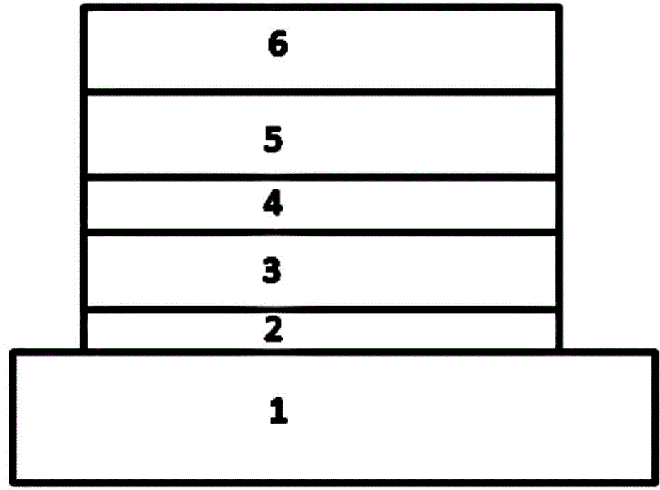
[0041] (2) Put the cleaned glass substrate into the sputtering equipment and use the Mo target to deposit the Mo back electrode layer, and set the sputtering background vacuum to 1×10 -4 Pa, process gas pressure 0.8Pa, target distance 80mm, power density 2W cm -2 , the film thickness is 800nm;
[0042] (3) Rotate the glass substrate prepared with the Mo back electrode layer to the next target position to prepare the light absorbing layer, which is divided into the following stages: ①Use the CIGS quadruple single target sputtering to deposit the CIGS light absorbing layer, and the target composition is Cu 0.25 In 0.18 Ga 0.06 Se 0.51 , and turn on the Ga co-sputtering target at the same time, the sputtering time i...
Embodiment 2
[0047] (1) After ultrasonically cleaning the glass substrate with tap water, deionized water, absolute alcohol, and acetone for 10 minutes, put the glass substrate in an oven and dry it at 100°C;
[0048] (2) Put the cleaned glass substrate into the sputtering equipment and use the MoCu alloy target to co-sputter to deposit the MoCu back electrode layer, and the sputtering background vacuum is set to 1×10 -4 Pa, process gas pressure 1Pa, target distance 60mm, power density 1.5W cm -2 , the film thickness is 600nm;
[0049] (3) Rotate the glass substrate prepared with the MoCu back electrode layer to the next target position to prepare the light-absorbing layer, which is divided into the following stages: ①Use the CIGS quadruple single-target sputtering to deposit the CIGS light-absorbing layer, and the target composition is Cu 0.25 In 0.18 Ga 0.06 Se 0.51 , and at the same time turn on the Ga co-sputtering target, the sputtering time is 10 minutes; ② turn off the co-sputt...
Embodiment 3
[0054] (1) After ultrasonically cleaning the glass substrate with tap water, deionized water, absolute alcohol, and acetone for 10 minutes, put the glass substrate in an oven and dry it at 100°C;
[0055] (2) Put the cleaned glass substrate into the sputtering equipment and use the Mo target to co-sputter to deposit the Mo back electrode layer, and the sputtering background vacuum is set to 1×10 -4 Pa, process gas pressure 0.6Pa, target distance 100mm, power density 2W cm -2 , the film thickness is 500nm;
[0056] (3) Rotate the glass substrate prepared with the Mo back electrode layer to the next target position to prepare the light absorbing layer, which is divided into the following stages: ①Use the CIGS quadruple single target sputtering to deposit the CIGS light absorbing layer, and the target composition is Cu 0.25 In 0.18 Ga 0.06 Se 0.51 , and turn on the CuGa co-sputtering target at the same time, the sputtering time is 10 minutes; ② turn off the co-sputtering tar...
PUM
| Property | Measurement | Unit |
|---|---|---|
| thickness | aaaaa | aaaaa |
| thickness | aaaaa | aaaaa |
| thickness | aaaaa | aaaaa |
Abstract
Description
Claims
Application Information
 - Generate Ideas
- Intellectual Property
- Life Sciences
- Materials
- Tech Scout
- Unparalleled Data Quality
- Higher Quality Content
- 60% Fewer Hallucinations
Browse by: Latest US Patents, China's latest patents, Technical Efficacy Thesaurus, Application Domain, Technology Topic, Popular Technical Reports.
© 2025 PatSnap. All rights reserved.Legal|Privacy policy|Modern Slavery Act Transparency Statement|Sitemap|About US| Contact US: help@patsnap.com


