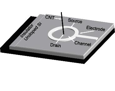
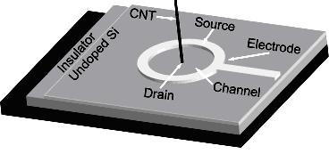
CNT (carbon nano tube) field emission array with current limiting transistors and preparation thereof
A carbon nanotube and field emission technology, which is applied in the manufacture of discharge tubes/lamps, parts of discharge tubes/lamps, cold cathodes, etc., can solve the problems of small total emission current, serious emission stability and uniformity, Emission performance cannot meet the requirements of the device, etc., to achieve the effect of high emission stability and high emission current density
- Summary
- Abstract
- Description
- Claims
- Application Information
AI Technical Summary
Problems solved by technology
Method used
Image

Examples
Embodiment
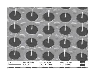
[0040] Embodiment: The process of preparing a carbon nanotube array with a flow-limiting field effect tube based on an SOI substrate is as follows:
[0041] (1) Firstly, the SOI substrate was ultrasonically cleaned in acetone and IPA for two minutes, and then PMMA electron beam photoresist was spin-coated on the substrate, followed by electron beam lithography, and the photolithographic pattern was a dot with a diameter of 100nm.
[0042] (2) Develop the substrate sample that has been subjected to electron beam lithography (such as placing it in MIBK for development), so that a photoresist mask with a circular hole pattern is formed on the surface of the substrate.
[0043] (3) The magnetron sputtering method is used to sputter the catalyst layer on the surface of the sample, which is composed of two layers of films. The lower layer is an ITO film with a thickness of 20nm; the upper layer is a nickel (Nickel) film with a thickness of 7nm.
[0044] (4) Next, the sample was immers...
PUM
 Abstract
Description
Claims
Application Information
 - R&D
- Intellectual Property
- Life Sciences
- Materials
- Tech Scout
- Unparalleled Data Quality
- Higher Quality Content
- 60% Fewer Hallucinations
Browse by: Latest US Patents, China's latest patents, Technical Efficacy Thesaurus, Application Domain, Technology Topic, Popular Technical Reports.
© 2025 PatSnap. All rights reserved.Legal|Privacy policy|Modern Slavery Act Transparency Statement|Sitemap|About US| Contact US: help@patsnap.com