
Method for correcting failures of quiescent current in aluminum gate CMOS

An oxide semiconductor and quiescent current technology, which is applied in semiconductor/solid-state device manufacturing, circuits, transistors, etc., can solve problems such as quiescent current failure, achieve the effect of increasing substrate surface concentration and improving quiescent current failure

Inactive Publication Date: 2011-06-29
PEKING UNIV FOUNDER GRP CO LTD +1
View PDF5 Cites 2 Cited by
  • Summary
  • Abstract
  • Description
  • Claims
  • Application Information

AI Technical Summary

Problems solved by technology

[0004] The purpose of the present invention is to provide a method for improving the quiescent current failure of the aluminum gate complementary metal oxide semiconductor for the defects of the existing aluminum gate complementary metal oxide semiconductor, thereby improving the working performance of the complementary metal oxide semiconductor

Method used


Image

  • Method for correcting failures of quiescent current in aluminum gate CMOS
  • Method for correcting failures of quiescent current in aluminum gate CMOS
  • Method for correcting failures of quiescent current in aluminum gate CMOS

Examples


Embodiment Construction

[0024] The present invention will be described in detail below in conjunction with the accompanying drawings and embodiments.

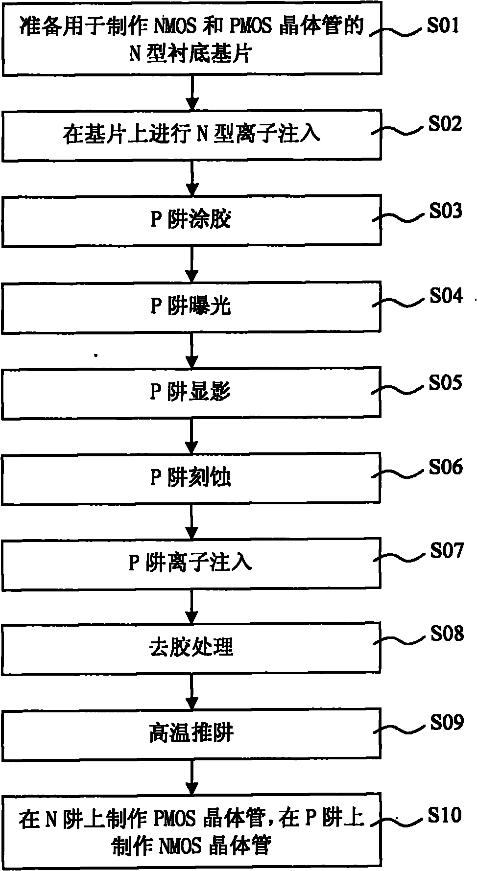
[0025] Such as figure 1 As shown, the method for improving the quiescent current failure of aluminum gate CMOS provided by the present invention is an improvement based on the P-well CMOS manufacturing process, and specifically includes the following steps:

[0026] In step S01 , prepare an N-type substrate substrate for fabricating aluminum gate CMOS (including NMOS and PMOS transistors), and the substrate is an N-type silicon wafer.

[0027] Step S02, performing N-type ion implantation on the substrate to increase the concentration of the substrate. N-type ion implantation uses P- ions; the energy range of ion implantation is 100Kev to 160Kev; the dose range of ion implantation is 2E11cm -2 to 4E11cm -2 .

[0028] Step S03 , performing P well glue coating on the substrate after N-type ion implantation. Use the centrifugal force generated when ...


PUM


Abstract

The invention relates to the manufacture technology of aluminum gate CMOSs (complementary metal oxide semiconductor), in particular to a method for correcting failures of quiescent current in an aluminum gate CMOS. The method is improved on the basis of the traditional manufacture technology of the aluminum gate CMOSs and comprises the step of conducting primary implantation technology of N-shaped irons to increase the surface concentration of the substrate after preparation of an N-shaped substrate. N-shaped irons implanted in the substrate form N wells automatically on the substrate during the diffusion process of a high-temperature furnace tube, so that the influence of the substrate concentration change on the electricity leakage of a PMOS (P-channel metal oxide semiconductor) tube can be reduced and the purpose of correcting failures of quiescent current in a circuit can be achieved.

Description

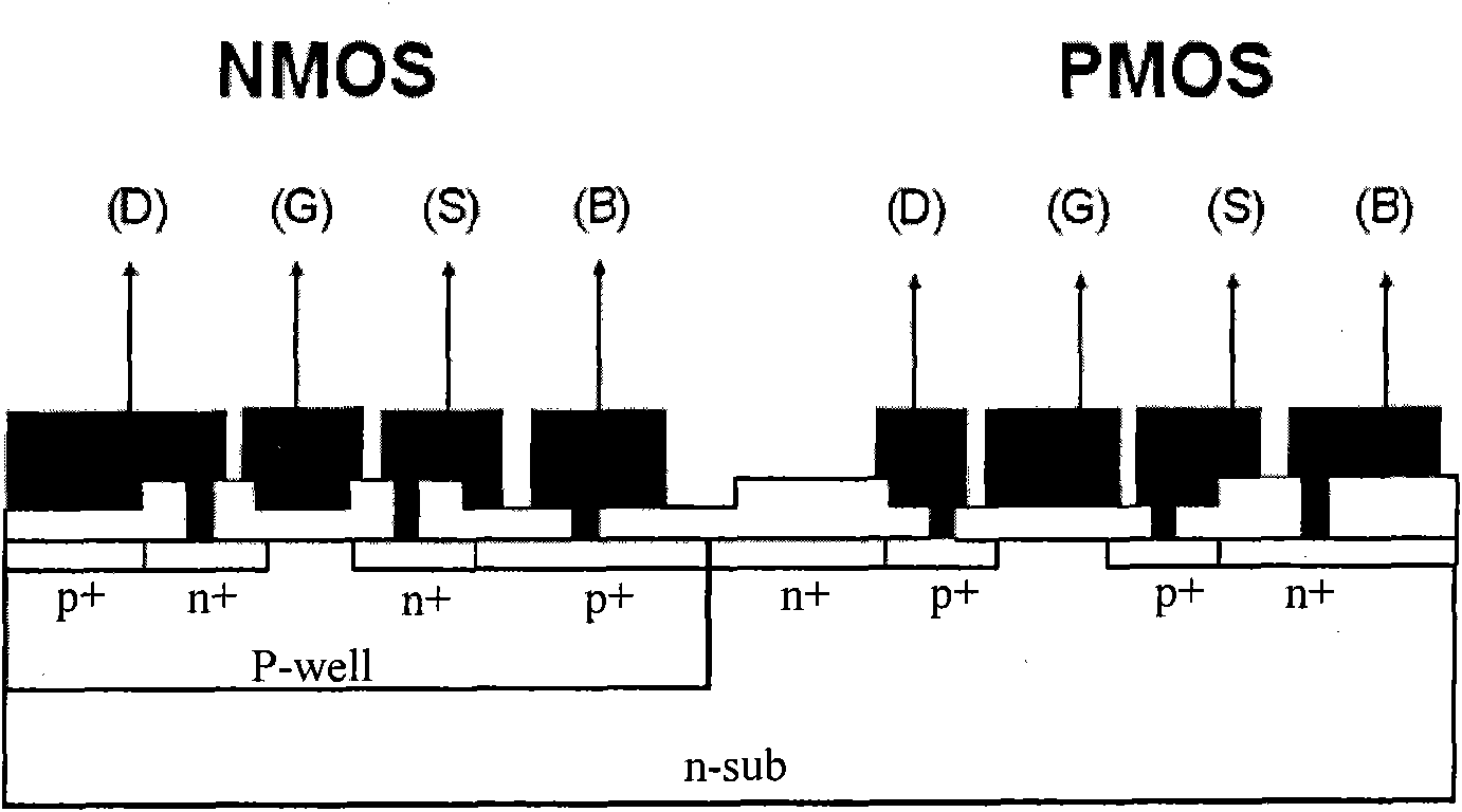
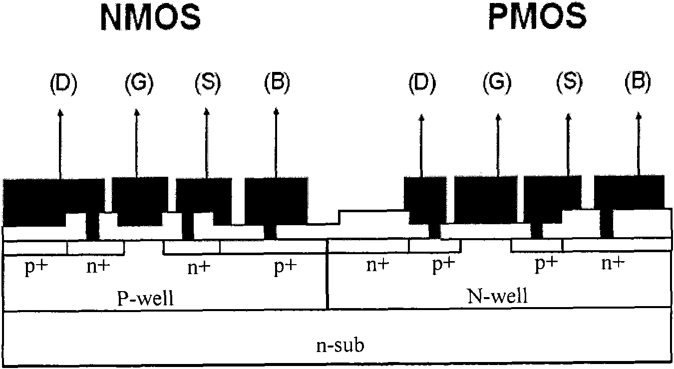
technical field [0001] The invention relates to a manufacturing process of aluminum gate complementary metal oxide semiconductors, in particular to a method for improving static current failure of aluminum gate complementary metal oxide semiconductors. Background technique [0002] Complementary Metal-Oxide Semiconductor (CMOS) is a voltage-controlled amplifying device, which is a raw material widely used in the manufacture of integrated circuit chips. CMOS is composed of PMOS (P-type oxide semiconductor) and NMOS (N-type oxide semiconductor). PMOS and NMOS are completely similar in structure, but the difference is the doping type of the substrate and source and drain. Simply put, PMOS is formed on an N-type silicon substrate by selective doping to form a P-type doped region as the source and drain regions of PMOS; NMOS is formed on a P-type silicon substrate by selective doping The N-type doped region is used as the source and drain regions of the NMOS. The manufacturing ...

Claims


Application Information

Patent Timeline
Patent Type & Authority Applications(China)
IPC IPC(8): H01L21/8238H01L27/092
Inventor 谭灿健谭志辉
Owner PEKING UNIV FOUNDER GRP CO LTD
Learn More