A pellicle for lithography
一种防尘薄膜组件、防尘薄膜的技术,应用在用于光机械处理的原件、光学、电气元件等方向,能够解决剥离困难、粘接剂老化加快等问题,达到容易更换、耐光性高、抑制老化的效果
- Summary
- Abstract
- Description
- Claims
- Application Information
AI Technical Summary
Problems solved by technology
Method used
Image
Examples
Embodiment 1
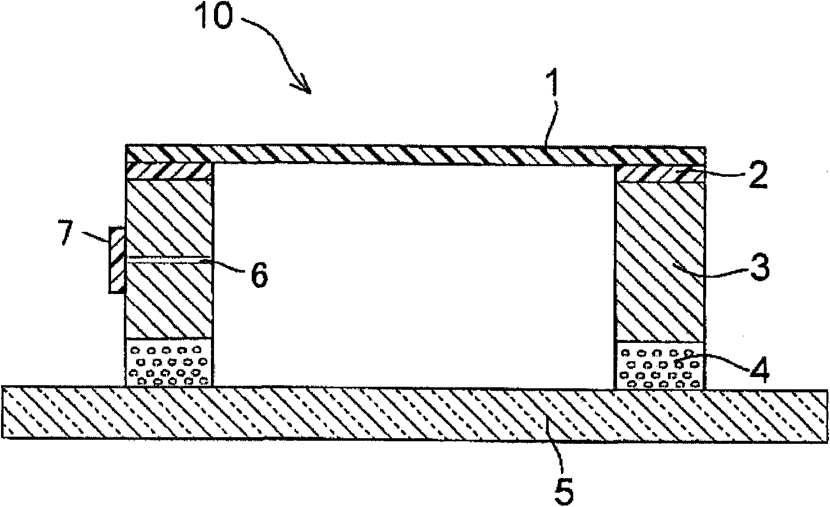
[0044] After cleaning the aluminum alloy pellicle frame (outer dimensions 149 mm x 113 mm x 4.5 mm, thickness 2 mm) with pure water, the Shin-Etsu Chemical Co., Ltd. A curable composition of a fluorine compound (trade name: X-71-8023) to form an adhesive layer. Next, heat is applied to the frame of the dust-proof film assembly by electromagnetic induction heating method, so that the curable composition is cured. The penetration of the adhesive layer after curing according to ASTM D-1403 was 100, and its thickness was 0.3 mm.
[0045] Apply Cytop (CYTOP) adhesive (trade name: CTX-A) manufactured by Asahi Glass Co., Ltd. on the other surface of the pellicle frame (the surface opposite to the surface on which the adhesive layer has been formed), Thus forming an adhesive layer. Heat was applied to the pellicle frame at a temperature of 130°C to cure the adhesive layer.
[0046] Then, attach the adhesive layer coated on the other side surface of the pellicle frame to the pellicl...
Embodiment 2
[0050] After washing the dust-proof film module frame made of aluminum alloy (outer dimension: 149mm × 113mm × 4.5mm, thickness: 2mm) with pure water, the surface of one side is coated with linear perfluorinated A curable composition of the compound (trade name: SIFEL8070 (Sifel 8070)) was used to form an adhesive layer. Then, the surface of the adhesive layer was contacted with a PET film. Next, the frame of the dust-proof film module is heated by electromagnetic induction heating, and after the curable composition in the adhesive layer is cured, the PET film is peeled off. After curing, the penetration of the adhesive layer defined by ASTM D-1403 was 70, and its thickness was 0.3 mm.
[0051] On the other surface of the pellicle frame (the surface opposite to the surface on which the adhesive layer has been formed), Cytop (CYTOP) adhesive (trade name: CTX-A) manufactured by Asahi Glass Co., Ltd. is applied, thereby Form an adhesive layer. Heat was applied to the pellicle ...
Embodiment 3
[0056] After cleaning the dust-proof film module frame made of aluminum alloy (outer dimension: 149mm × 113mm × 4.5mm, thickness: 2mm) with pure water, the surface of one side is coated with linear perfluorinated film made by Shin-Etsu Chemical Co., Ltd. Compound curable composition (trade name: X-71-8122) to form an adhesive layer. Then, the surface of the adhesive layer was contacted with a PET film. Next, the frame of the dust-proof film module is heated by electromagnetic induction heating method, and after the curable composition in the adhesive layer is cured, the PET film is peeled off. After curing, the penetration of the adhesive layer defined by ASTM D-1403 was 70, and its thickness was 0.3 mm.
[0057] Apply Cytop (CYTOP) adhesive (trade name: CTX-A) manufactured by Asahi Glass Co., Ltd. on the other surface of the pellicle frame (the surface opposite to the surface on which the adhesive layer has been formed), An adhesive layer was thus formed, and the pellicle f...
PUM
| Property | Measurement | Unit |
|---|---|---|
| wavelength | aaaaa | aaaaa |
| wavelength | aaaaa | aaaaa |
| surface smoothness | aaaaa | aaaaa |
Abstract
Description
Claims
Application Information
 - Generate Ideas
- Intellectual Property
- Life Sciences
- Materials
- Tech Scout
- Unparalleled Data Quality
- Higher Quality Content
- 60% Fewer Hallucinations
Browse by: Latest US Patents, China's latest patents, Technical Efficacy Thesaurus, Application Domain, Technology Topic, Popular Technical Reports.
© 2025 PatSnap. All rights reserved.Legal|Privacy policy|Modern Slavery Act Transparency Statement|Sitemap|About US| Contact US: help@patsnap.com


