
Semiconductor package for printing bonding material on lead frame and wafer and manufacturing method thereof

A lead frame and bonding material technology, used in semiconductor/solid-state device manufacturing, semiconductor devices, semiconductor/solid-state device components, etc., can solve the problems of chip cracks, small chip size, high stress, etc.

Active Publication Date: 2013-09-18
重庆万国半导体科技有限公司
View PDF0 Cites 0 Cited by
  • Summary
  • Abstract
  • Description
  • Claims
  • Application Information

AI Technical Summary

Problems solved by technology

[0008] 1. In the same package size, since the adhesive material (solder paste or epoxy resin) is first laid on the carrier table by dispensing, when the chip is attached and bonded on it, the adhesive material will Spilling from around the chip, due to the unavoidable spillover effect, will result in a smaller packaged chip size
[0009] 2. The adhesive material (solder paste or epoxy resin) used to bond the chip is formed by dispensing and laying on the carrier table. This method will cause the thickness of the formed adhesive material to be uneven. This will cause the chip to be attached to it to tilt
[0010] 3. Using solder paste or epoxy resin as the bonding material to bond the chip to the carrier table will generate high stress, which will easily lead to cracks in the chip
[0012] 5. In the process of bonding chips, if solder paste or eutectic material is used as the bonding material, a higher process operating temperature is required, which will lead to rapid oxidation of the lead frame
[0013] 6. The epoxy resin formed by dispensing method has low electrical conductivity and thermal conductivity

Method used


Image

  • Semiconductor package for printing bonding material on lead frame and wafer and manufacturing method thereof
  • Semiconductor package for printing bonding material on lead frame and wafer and manufacturing method thereof
  • Semiconductor package for printing bonding material on lead frame and wafer and manufacturing method thereof

Examples


Embodiment 1

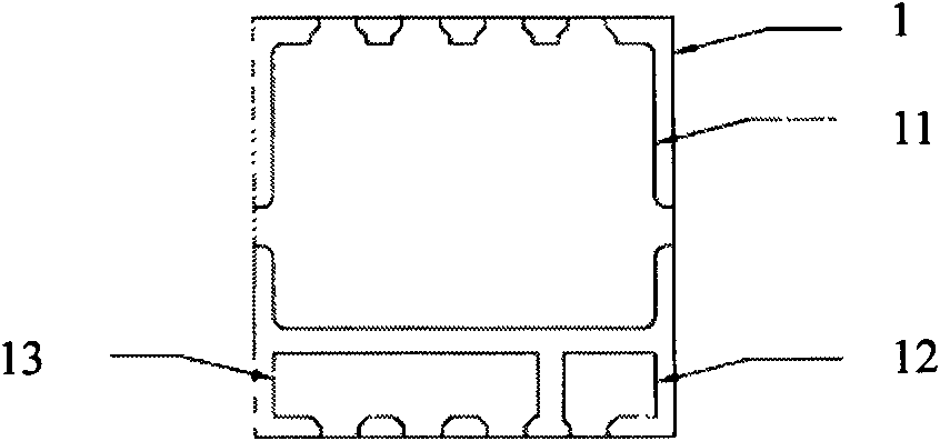
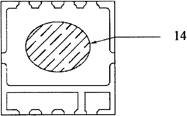
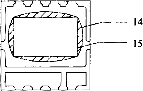
[0100] Such as Figure 2E As shown, it is a schematic structural diagram of a semiconductor package for printing adhesive materials on a lead frame provided in this embodiment, which includes: a chip stage 21 and pins 21' electrically connected to the chip stage 21 , and a lead frame 2 with two pins 22 and 23 electrically isolated from the stage 21 (such as Figure 2A shown); and a MOSFET 25 having a top gate and a top source (not shown) on its upper surface and a bottom drain (not shown) on its back. The bottom drain of the MOSFET 25 is bonded to the wafer stage 21 , and the top gate and top source of the MOSFET 25 are bonded to pins 22 and 23 respectively through several metal leads 26 . Wherein, the printing adhesive material 24 formed by printing (such as Figure 2B shown), and the printed bonding material 24 and the MOSFET 25 have the same size and shape, by Figure 2C It can be seen that the MOSFET 25 completely covers the printed adhesive material 24 . The adhesive ...

Embodiment 2

[0103] Such as Figure 3A-3E As shown, there is provided another specific embodiment of the semiconductor package in which the adhesive material is printed on the lead frame of the present invention. its with Figure 2A-2E The illustrated embodiment is similar, and the only difference is that the printed bonding material 34 formed in this embodiment and the chip stage 31 on the lead frame 3 have the same size and shape (such as Figure 3B shown), by Figure 3C It can be seen that when the MOSFET 35 is pasted on the printed adhesive material 34 , a part of the surrounding area of ​​the slide table 31 where the adhesive material 34 is printed is still exposed. Afterwards, it is the same as the process described in Example 1, as Figure 3D As shown, a number of metal leads 36 are respectively connected to the front electrode of MOSFET 35 and pins 32 and 33 by wire bonding technology to form connection bonds between MOSFET 35 and pins 32 and 33 . Such as Figure 3E As shown, ...

Embodiment 3

[0105] Such as Figures 4A-4E As shown, there is provided another specific embodiment of the semiconductor package in which the adhesive material is printed on the lead frame of the present invention. its with Figure 2A-2E and the embodiments shown in 3A to 3E are similar, and the only difference is that the printed bonding material 44 formed in this embodiment has the same shape and slightly larger size than the MOSFET 45. Figure 4B and 4C It can be seen that when the MOSFET 45 is pasted on the printed adhesive material 44, there is still a very small area of ​​the printed adhesive material 44 exposed around it. Afterwards, the process described in Example 1 and Example 2 is the same, as Figure 4D As shown, a number of metal leads 46 are respectively connected to the front electrode of MOSFET 45 and pins 42 and 43 by wire bonding technology to form connection bonds between MOSFET 45 and pins 42 and 43 . Such as Figure 4E As shown, the lead frame 4, MOSFET 45 and meta...


PUM


Abstract

The invention provides a semiconductor package for printing a bonding material on a lead frame and a wafer and a manufacturing method thereof. In the invention, the bonding material is printed on a chip carrying table and a pin of the lead frame; the bonding material is also printed on a positive electrode of a semiconductor chip; hereafter, the back of the semiconductor chip is bonded on the chip carrying table; and the positive electrode of the semiconductor chip is connected with the pin by using a metal connector, wherein the size, the shape and the thickness of the bonding material are determined according to actual demand or the bonded semiconductor chip and the contact area of the metal connector. The semiconductor package provided by the invention overcomes the obvious disadvantages and defects in the prior art by utilizing the characteristics of the printed bonding material, and can effectively improve the quality and the performance of the semiconductor products and enhance the production efficiency.

Description

technical field [0001] The invention belongs to the field of integrated circuit packaging, and relates to a semiconductor packaging process; specifically, it refers to a semiconductor packaging for printing adhesive materials on a lead frame and a wafer and a manufacturing method thereof. Background technique [0002] In the packaging of integrated circuits, a lead frame is a substrate that provides chip support and is made of copper or alloys. The lead frame has the following characteristics: good ductility, high strength, easy forming, excellent coating performance, good corrosion and oxidation resistance, high electrical conductivity and high thermal conductivity, and can be well bonded to plastic packages , and has a thermal expansion coefficient very close to that of the chip and the plastic package. The lead frame includes a carrier table for bonding the chip, and several pins for connecting the chip to external components; among them, it is first necessary to use a m...

Claims


Application Information

Patent Timeline
Patent Type & Authority Patents(China)
IPC IPC(8): H01L23/495H01L23/488H01L21/50H01L21/48H01L21/60
CPCH01L2224/48247H01L2224/49111H01L2224/49175H01L2924/13091H01L2224/45144H01L2924/01322H01L2924/181H01L2224/40245H01L24/40H01L2224/4103H01L2924/14H01L2224/371H01L2224/37H01L2224/40H01L2224/41H01L2224/73221H01L2924/00014H01L2924/00H01L2924/00012
Inventor 张晓天鲁军刘凯
Owner 重庆万国半导体科技有限公司
Learn More