Integrated circuit layout structure and manufacturing method thereof

A layout structure and integrated circuit technology, which is applied to circuits, electrical components, and electrical solid devices, can solve problems such as uneven copper metal thickness of wide and thin lines, improve planarization capabilities, avoid hot spots, and reduce burdens Effect

Inactive Publication Date: 2010-11-17
INST OF MICROELECTRONICS CHINESE ACAD OF SCI
View PDF0 Cites 6 Cited by
  • Summary
  • Abstract
  • Description
  • Claims
  • Application Information

AI Technical Summary

Problems solved by technology

[0006] In order to solve the problem of non-uniform copper metal thickness of wide lines and thin lines of integrated circuit layout after chemical mechanical polishing in the prior art, the main purpose of the present invention is to provide an integrated circuit layout structure and its manufacturing method

Method used


Image

  • Integrated circuit layout structure and manufacturing method thereof
  • Integrated circuit layout structure and manufacturing method thereof
  • Integrated circuit layout structure and manufacturing method thereof

Examples


Embodiment Construction

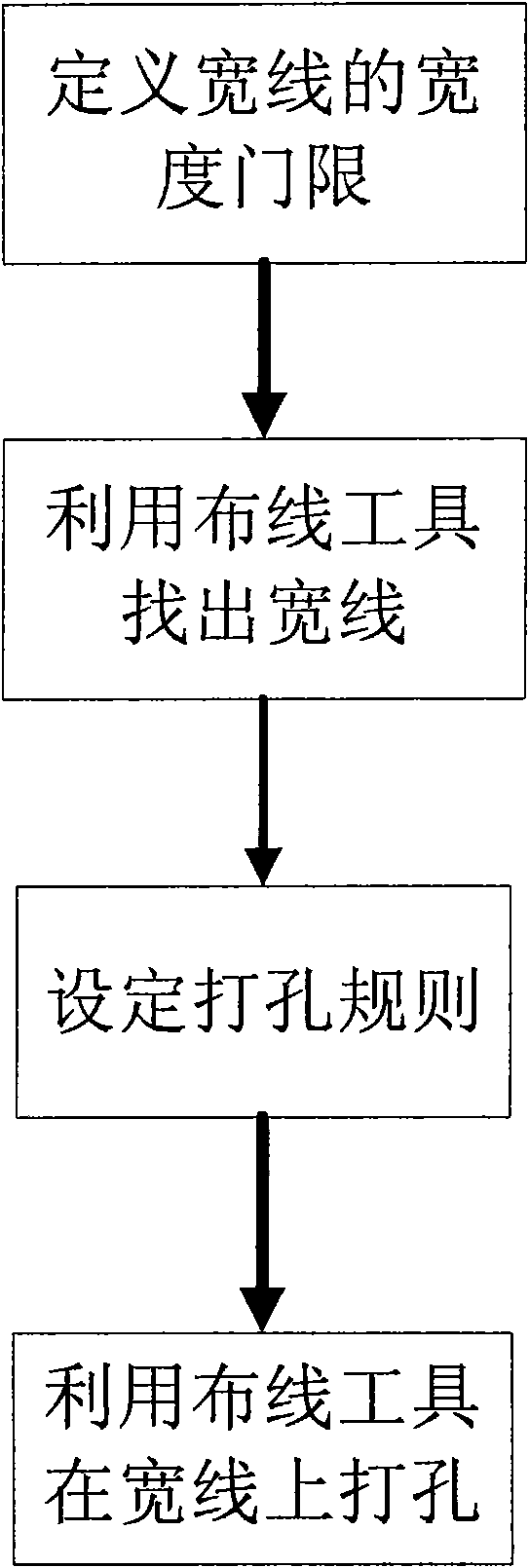
[0028] In order to make the object, technical solution and advantages of the present invention clearer, the present invention will be further described in detail below in conjunction with specific embodiments and with reference to the accompanying drawings.

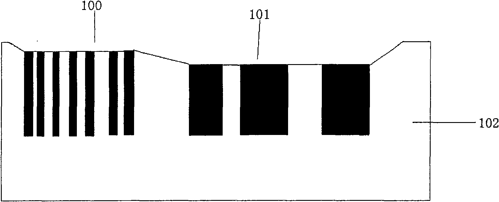
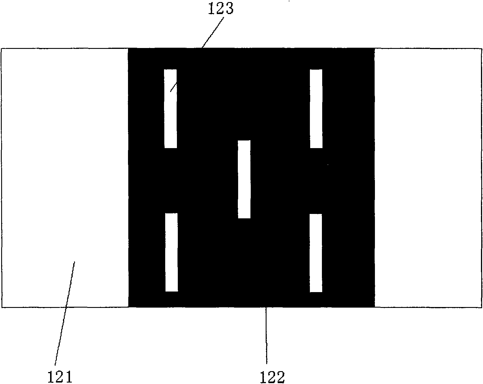
[0029] see figure 2 , figure 2 A top view of an integrated circuit layout structure is proposed for the present invention. The integrated circuit layout structure provided by the present invention includes: a dielectric; a wide copper wire grown in the dielectric, and a wide copper wire is a copper wire with a width greater than a certain threshold; and a wide copper wire grown on the wide copper wire. Evenly distributed small holes are punched. The small holes punched on the wide copper wire shall adopt the minimum wire width and be evenly distributed on the copper wire. The wide line of holes reduces the removal rate of copper in chemical mechanical polishing. This structure makes the growth of copper in wide and ...


PUM


Abstract

The invention relates to the fields of an integrated circuit manufacturing process and layout design, and discloses an integrated circuit layout structure and a manufacturing method thereof. In order to solve the problem of too low thickness of copper metal in a broad-line region of an integrated circuit layout after chemically mechanical polishing in the prior art, the invention provides an integrated circuit layout structure and a preparation method thereof. By regularly drilling holes for broad lines and through chemically mechanical polishing, the thickness of the copper metal of the broad lines is greatly improved, and the thickness of the copper metal on the broad lines and the thin lines is uniform, so the burden of the chemically mechanical polishing is lightened, the planization capacity is improved, the hotspot problems caused by the broad lines are avoided, and the finished product rate is improved.

Description

technical field [0001] The invention relates to the technical field of integrated circuit manufacturing technology and layout design, in particular to an integrated circuit layout structure and a manufacturing method thereof. Background technique [0002] Chemical Mechanical Polishing (CMP) is a surface planarization process used in the manufacture of integrated circuits. It is a combined technology of chemical corrosion and mechanical polishing. Forming a smooth and flat surface on the surface of the medium is recognized as the best material global planarization method in the VLSI stage. This method can not only obtain a more perfect surface, but also obtain a higher polishing rate. Integrated Circuit (IC) manufacturing technology develops at a speed of doubling the integration level every 18 months according to Moore's Law, but when the feature size of integrated circuits drops below 90 nanometers, IC manufacturing technology encounters unprecedented challenges , chemical...

Claims


Application Information

Patent Timeline
Patent Type & Authority Applications(China)
IPC IPC(8): H01L23/522H01L21/768H01L21/321
Inventor 文鼎童陈岚阮文彪李志刚
Owner INST OF MICROELECTRONICS CHINESE ACAD OF SCI
Why Eureka
Try Eureka