GaN-based LED having nanometer structure inserted layer
A nanostructure and insertion layer technology, applied in electrical components, circuits, semiconductor devices, etc., can solve the problems of reducing the light-emitting area of nanostructures, generating thermal effects, and P-type damage.
- Summary
- Abstract
- Description
- Claims
- Application Information
AI Technical Summary
Problems solved by technology
Method used
Image
Examples
Embodiment Construction
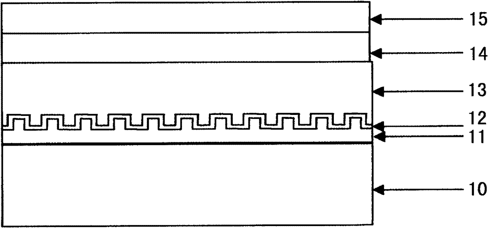
[0027] The present invention provides a GaN-based LED with a nanostructure insertion layer, comprising:
[0028] A substrate 10, the substrate 10 is made of silicon, sapphire, gallium nitride, gallium arsenide or silicon carbide;
[0029] A nanostructure template 11, the nanostructure template 11 is epitaxially grown on the substrate 10, the surface of the nanostructure template 11 is in a concave-convex shape, and the nanostructure template 11 on the concave-convex surface is obtained by electron beam exposure, holographic lithography, and two The porous alumina structure formed by step oxidation, the self-organized structure formed by metal under annealing conditions or the structure formed by silica nanoparticles is used as a mask to etch by dry etching method, or directly etched by focused ion beam wherein the surface of the nanostructure template 11 is a columnar structure, and the shape is a cylinder, a hexagonal prism, a square prism, a rhombus prism, a cubic prism, a t...
PUM
 Abstract
Description
Claims
Application Information
 - R&D
- Intellectual Property
- Life Sciences
- Materials
- Tech Scout
- Unparalleled Data Quality
- Higher Quality Content
- 60% Fewer Hallucinations
Browse by: Latest US Patents, China's latest patents, Technical Efficacy Thesaurus, Application Domain, Technology Topic, Popular Technical Reports.
© 2025 PatSnap. All rights reserved.Legal|Privacy policy|Modern Slavery Act Transparency Statement|Sitemap|About US| Contact US: help@patsnap.com


