Electrostatic protection circuit and display device adopting same
An electrostatic protection and circuit technology, applied in the direction of circuits, electrical components, electric solid devices, etc., can solve the problem of not being able to increase the load of the gate drive circuit and source drive circuit, and achieve stable and reliable performance without permanent damage Effect
- Summary
- Abstract
- Description
- Claims
- Application Information
AI Technical Summary
Problems solved by technology
Method used
Image


Examples
no. 1 example
[0053] Figure 5 It is an electrostatic protection circuit according to an embodiment of the present invention. Please refer to Figure 5 , the electrostatic protection circuit 500 includes a transistor 502 , a transistor 504 , a transistor 506 , a voltage dividing circuit 508 and a voltage dividing circuit 510 . In this example, each of the aforementioned transistors is an n-type metal-oxide-semiconductor field-effect transistor. Preferably, the channel width of the transistor 504 is equal to that of the transistor 506 , and the channel width of the transistor 502 is much larger than that of the transistor 504 (for example, the ratio is 10:1).
[0054] One source / drain of the transistor 502 is coupled to the power line 520 , and the other source / drain is coupled to the power line 530 . One source / drain of the transistor 504 is coupled to the power line 520 , and the other source / drain is coupled to the gate of the transistor 502 . One source / drain of the transistor 506 is...
no. 2 example
[0068] Figure 9 It is an electrostatic protection circuit according to another embodiment of the present invention. exist Figure 9 In, the label and Figure 5 Those with the same reference number in are denoted as the same object. Please refer to Figure 9 , this ESD protection circuit 900 with Figure 5 The difference of the ESD protection circuit 500 shown is that the transistor 902 , the transistor 904 and the transistor 906 in the ESD protection circuit 900 are all P-type MOSFETs. Preferably, the channel width of the transistor 904 is equal to that of the transistor 906 , and the channel width of the transistor 902 is much larger than that of the transistor 904 (for example, the ratio is 10:1).
[0069] Each impedance in the ESD protection circuit 900 can be realized by a capacitor, as Figure 10 shown. Figure 10 for Figure 9 One of the implementation states of the electrostatic protection circuit shown. In the embodiment shown in the ESD protection circuit 10...
no. 3 example
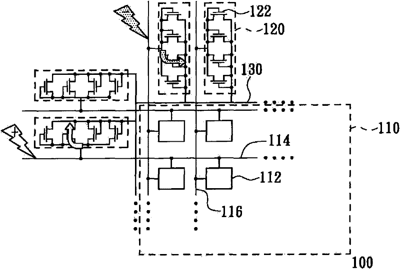
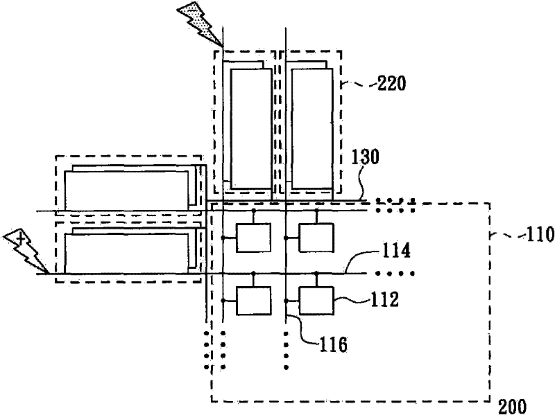
[0077] This embodiment is mainly to illustrate how to apply the electrostatic protection circuit of the present invention in a display device (such as a liquid crystal display device). Please refer to Figure 11 , which is an explanatory diagram of a display device according to an embodiment of the present invention. The display device 1100 includes a display panel 1110 , a plurality of electrostatic protection circuits 1120 and a short ring 1130 . The display panel 1110 includes a plurality of pixels 1112 , a plurality of gate lines 1114 and a plurality of source lines 1116 , and each pixel 1112 is coupled to one of the gate lines 1114 and one of the source lines 1116 .
[0078]Each ESD protection circuit 1120 is coupled to the short ring 1130 , and each ESD protection circuit 1120 is coupled to one of the gate lines 1114 and the source lines 1116 . Briefly, the gate lines 1114 and the source lines 1116 are regarded as the power lines 520 in the foregoing embodiments, and t...
PUM
 Abstract
Description
Claims
Application Information
 - R&D
- Intellectual Property
- Life Sciences
- Materials
- Tech Scout
- Unparalleled Data Quality
- Higher Quality Content
- 60% Fewer Hallucinations
Browse by: Latest US Patents, China's latest patents, Technical Efficacy Thesaurus, Application Domain, Technology Topic, Popular Technical Reports.
© 2025 PatSnap. All rights reserved.Legal|Privacy policy|Modern Slavery Act Transparency Statement|Sitemap|About US| Contact US: help@patsnap.com