
Industrialized production process of crystalline silicon solar battery

A solar cell and production process technology, applied in the field of solar cells, to achieve strong reflection, increase absorption, and reduce the probability of leakage

Active Publication Date: 2010-09-22
JA YANGZHOU SOLAR PHOTOVOLTAIC ENG
View PDF5 Cites 38 Cited by
  • Summary
  • Abstract
  • Description
  • Claims
  • Application Information

AI Technical Summary

Problems solved by technology

[0008] Although the above-mentioned methods can reduce the adverse effects of the double chemical etching of the silicon wafer, control the curvature of the battery, and reduce the generation of debris, it is still necessary to stack the silicon wafers together for edge etching, which cannot directly avoid the damage of the suede surface. possibility

Method used


Image

  • Industrialized production process of crystalline silicon solar battery
  • Industrialized production process of crystalline silicon solar battery
  • Industrialized production process of crystalline silicon solar battery

Examples


Embodiment 1

[0029] The industrial production process of crystalline silicon solar cells provided in this example is as follows: select silicon wafers, perform texturing on the front surface, phosphorus diffusion, removal of phosphosilicate glass formed on the surface during phosphorus diffusion, and silicon nitride deposition on the front surface by PECVD in sequence, The silicon wafer protected by the silicon nitride anti-reflection film on the front surface is placed in heated lye for back polishing to remove the diffusion layer on the back, and then cleaned and dried with anti-bending aluminum paste for screen printing and sintering.

[0030] The lye used during polishing is inorganic lye, which is an aqueous solution of sodium hydroxide or potassium hydroxide, with a weight percentage of 10-40% and a temperature of 50-90°C; organic lye can also be used for polishing. The lye, the organic lye is an aqueous solution of tetramethylammonium hydroxide or ethylenediamine, its weight percenta...

Embodiment 2

[0032] The industrial production process of crystalline silicon solar cells provided in this embodiment includes the following steps:

[0033] (1) Suede corrosion

[0034] Select a single-crystal silicon wafer with a resistivity of 1.0-5Ω·cm, put the two pieces together in a flower basket, and then place them in a hydrogen oxide with a temperature of 80-95°C and a volume percentage of 1-10% alcohol. Carry out one-sided etching of the front surface in sodium aqueous solution, the weight percentage of sodium hydroxide aqueous solution is 0.5-1.5%, soak the silicon wafer in 10% dilute hydrochloric acid for 2 minutes after making texture, then rinse it with deionized water, and set aside ;

[0035] (2) Phosphorus diffusion

[0036] Using phosphorus oxychloride liquid source, diffusion is carried out in an industrial tubular diffusion furnace, so that the temperature in the constant temperature zone is 800 ℃ ~ 900 ℃, the diffusion time is 30 ~ 50 minutes, and the diffusion square...

Embodiment 3

[0044] The industrial production process of crystalline silicon solar cells provided in this embodiment includes the following steps:

[0045] (1) Suede corrosion

[0046]Select a single-crystal silicon chip with a resistivity of 1.0-5Ω·cm, put the two pieces together in a flower basket, and then place them in a glass with a temperature of 80-95°C and a volume percentage of 1-10% isopropanol. The front surface is etched on one side in sodium hydroxide aqueous solution, the weight percentage of sodium hydroxide aqueous solution is 0.5-1.5%, the silicon chip after texturing is soaked in 10% dilute hydrochloric acid for 2 minutes, and then rinsed with deionized water ,spare;

[0047] (2) Phosphorus diffusion

[0048] Phosphorus oxychloride liquid source is used to diffuse in an industrial tubular diffusion furnace. The temperature in the constant temperature zone is 800℃~900℃, the diffusion time is 30~50min, and the diffusion resistance is controlled at 40~60Ω / □;

[0049] (3) ...


PUM

PropertyMeasurementUnit
Resistivityaaaaaaaaaa
Sheet resistanceaaaaaaaaaa
Film thicknessaaaaaaaaaa

Abstract

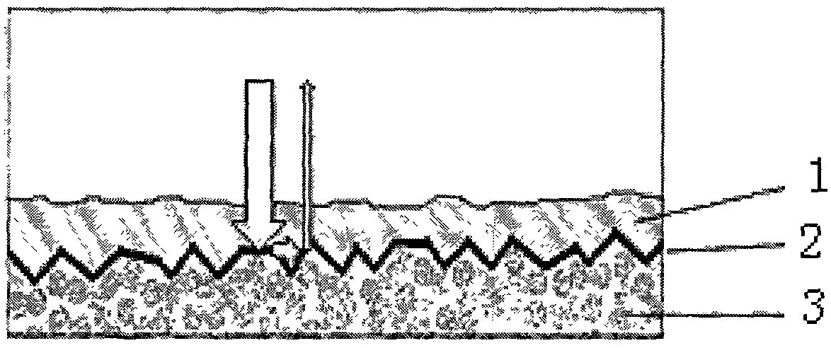
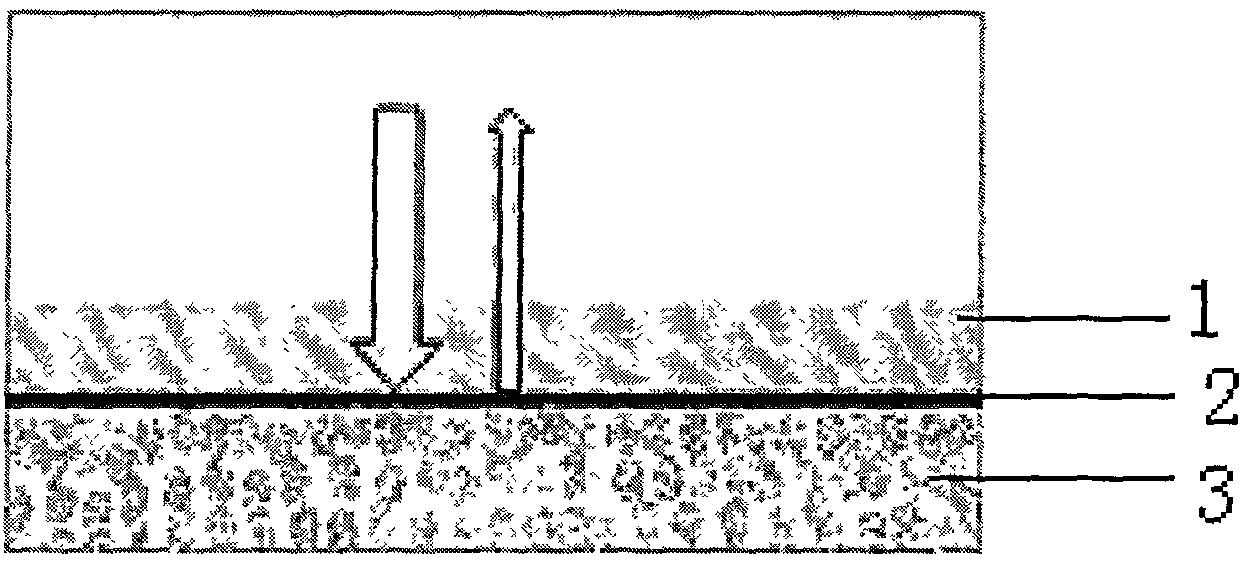
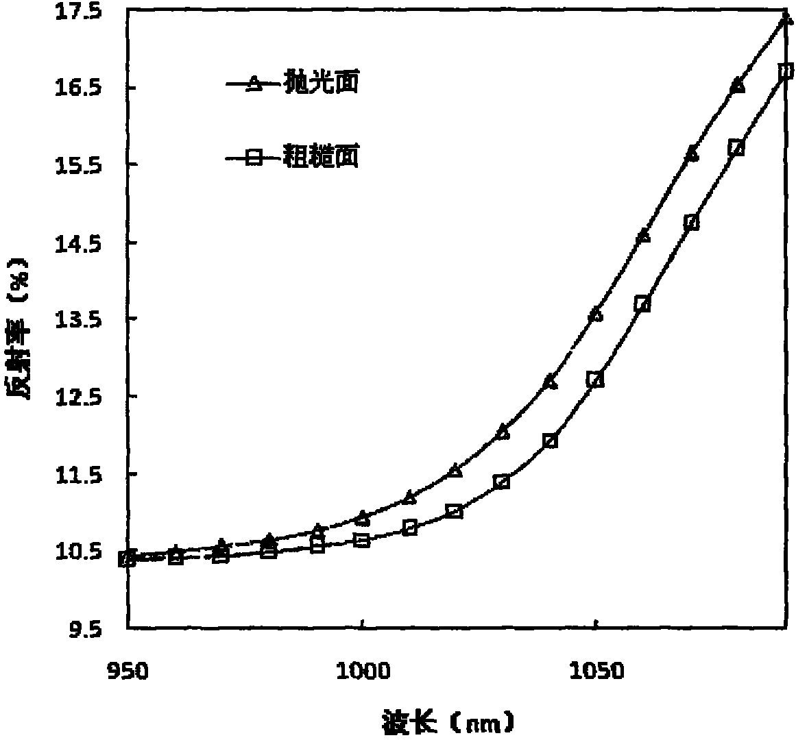
The invention discloses an industrialized production process of a crystalline silicon solar battery, which comprises the following steps of: selecting a silicon chip; performing front surface matte making, phosphorous diffusion, the removal of phosphorosilicate glass formed on the surface during the phosphorous diffusion, and the deposition of silicon nitride on the front surface through PECVD inturn, and then putting an anti-reflecting film protected silicon ship provided with the front surface silicon nitride into heated alkali liquor to perform back polishing so as to remove a diffusion layer on the back surface; and washing and drying the silicon chip, and printing and sintering the silicon chip by adopting a bending-resistant aluminum paste silk screen. The process adopts a chemicalmethod to replace a plasma etching process, realizes non-contact of a matte surface of the silicon chip in the whole production flow, avoids matte surface damages caused by silicon chip friction, so the probability of electric leakage after facade silver paste sintering is reduced; the flat and clean back surface is favorable for the reaction of aluminum and silicon during the sintering to form amore uniform aluminum back surface field; and a polished surface has a stronger reflex action compared with an irregular matte surface, and can increase the absorption of incident light, improve the spectral response of the long-wavelength of a battery chip, and significantly improve a short-circuit current and an open-circuit voltage.

Description

technical field [0001] The invention belongs to the technical field of solar cells, and in particular relates to an industrialized production process of crystalline silicon solar cells. Background technique [0002] With the decrease of fossil energy reserves and various environmental problems caused by the greenhouse effect, people's demand for new energy is getting stronger and stronger. As a photoelectric conversion device, solar cells are the most direct way to obtain solar energy. In recent years, the world output of solar cells has been growing at a high rate of 30% to 40% per year, becoming one of the fastest growing industries. [0003] At present, crystalline silicon solar cells are the mainstream of photovoltaic products, accounting for about 90% of the market share. Domestic crystalline silicon production lines are basically designed according to the battery production process of texturing, diffusion, plasma etching, phosphosilicate glass cleaning, silicon nitri...

Claims


Application Information

Patent Timeline
IPC IPC(8): H01L31/18
CPCY02P70/50
Inventor 尹海鹏朱生宾何胜金井升蒋秀林李玉庆单伟
Owner JA YANGZHOU SOLAR PHOTOVOLTAIC ENG
Learn More