Method for preparing semiconductor secondary grid-metal primary grid crystalline silicon solar battery
A technology for solar cells and semiconductors, applied in semiconductor devices, circuits, electrical components, etc., can solve the problems of complex manufacturing process and high cost, and achieve the effects of simple process, reduced raw material cost, and reduced usage
- Summary
- Abstract
- Description
- Claims
- Application Information
AI Technical Summary
Problems solved by technology
Method used
Image
Examples
Embodiment Construction
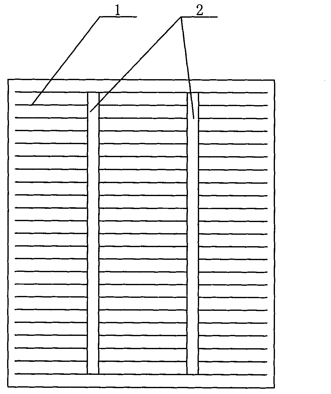
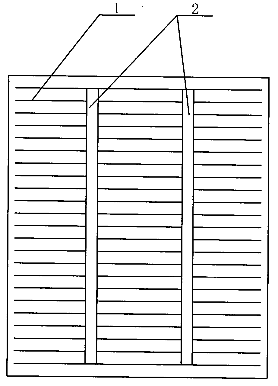
[0012] see figure 1 , this specific embodiment adopts the following technical scheme: it is composed of a plurality of semiconductor sub-gates 1 and several metal electrode busbars 2, and several metal electrode busbars connect a plurality of semiconductor sub-gates 1 to each other ; Its preparation method comprises the following steps: 1. Texturing the surface of the silicon chip, 2. Screen-printing thin lines of phosphorus paste, 3. Diffusion at high temperature to obtain thin grid lines with low sheet resistance and other emission areas with suitable sheet resistance, 4. Remove the peripheral or back PN junction, 5. Remove the phospho-silicate glass, 6. Coat the anti-reflection film, 7. Screen print the back electrode and the back aluminum paste and dry them. 8. Screen print the front silver paste main grid Line, nine, electrode co-sintering.
[0013] The square resistance of the plurality of semiconductor sub-gates 1 is less than 10 ohms, the line width is between 10-150 ...
PUM
 Abstract
Description
Claims
Application Information
 - R&D Engineer
- R&D Manager
- IP Professional
- Industry Leading Data Capabilities
- Powerful AI technology
- Patent DNA Extraction
Browse by: Latest US Patents, China's latest patents, Technical Efficacy Thesaurus, Application Domain, Technology Topic, Popular Technical Reports.
© 2024 PatSnap. All rights reserved.Legal|Privacy policy|Modern Slavery Act Transparency Statement|Sitemap|About US| Contact US: help@patsnap.com


