Integrated grating micro-cantilever biochemical sensor and chip manufacturing method
A biochemical sensor and micro-cantilever technology, applied in the field of micro-electromechanical systems and sensing, to achieve the effect of being suitable for mass production, high sensitivity and high sensitivity
- Summary
- Abstract
- Description
- Claims
- Application Information
AI Technical Summary
Problems solved by technology
Method used
Image
Examples
Embodiment 1
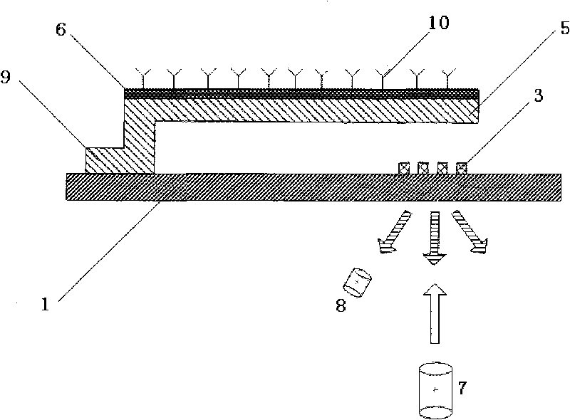
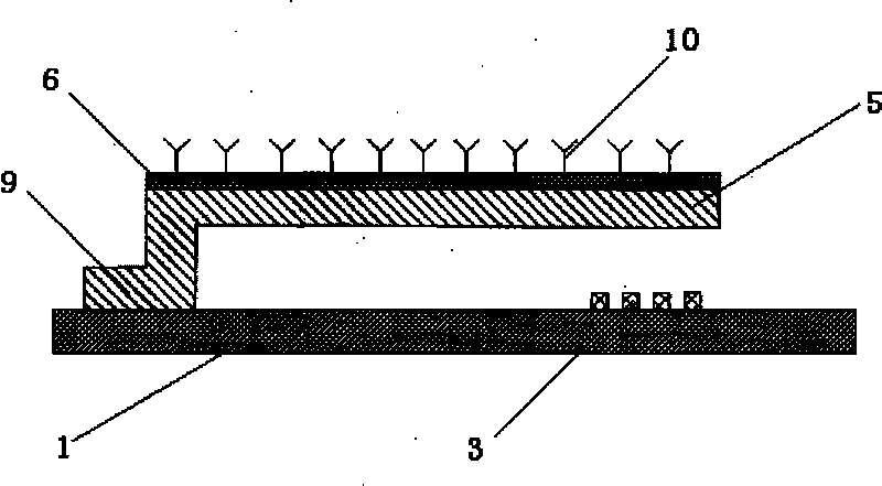
[0061] Sensor Structure Reference figure 2 , making the integrated grating micro-cantilever biochemical sensor of the present invention, its specific preparation steps are as follows:
[0062] 1). First clean the glass substrate, deposit gold on it by sputtering or evaporating a metal film, the thickness of which is: 0.1-0.5 microns; photoetch or corrode gold to form metal (gold) Grating, the metal grating has a width of 5 microns and a pitch of 5 microns;
[0063] 2) the glass substrate obtained in step 1) is coated with photoresist as a sacrificial layer, and the thickness of the photoresist is 6 microns, and photoetching forms the anchor pattern of the micro-cantilever beam;
[0064] 3) adopt the process of sputtering or vapor deposition metal film, then deposit aluminum and gold on the glass substrate obtained in step 2) to form the metal layer of the micro-cantilever beam and the metal layer forming the biochemical probe attachment layer, the thickness of aluminum is 2 ...
Embodiment 2
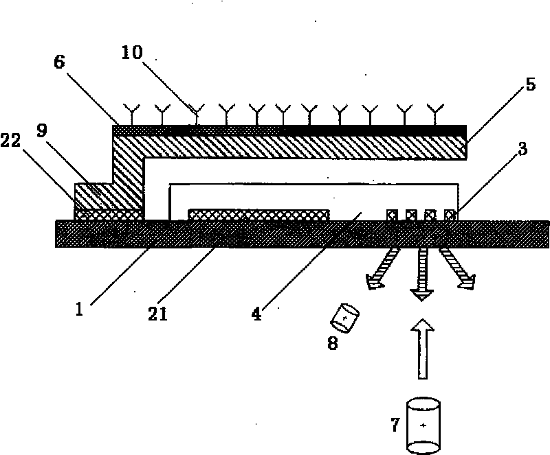
[0076] Sensor Structure Reference figure 2 , 3 , to make an integrated grating micro-cantilever biochemical sensor of the present invention, the specific preparation steps are as follows:
[0077] 1). First clean the glass sheet, apply photoresist on it, and photolithographically form electrodes, lead pads and grating patterns;
[0078] 2). Then, on the glass substrate obtained in step 1), chromium and gold are deposited by sputtering or vapor deposition of metal thin film. The thickness of chromium is 8 nanometers, and the thickness of gold is 100 nanometers; process to form electrodes, lead pads and gratings; the gratings have a width of 3 microns and a pitch of 3 microns;
[0079] 3) On the glass substrate obtained in step 2), use PECVD to deposit 200 nanometers of thick silicon dioxide as an insulating layer, coat photoresist on it, and photolithography to form a pattern, corrode silicon dioxide, and expose the micro-cantilever anchor point and Pressure solder block. ...
Embodiment 3
[0094] Sensor Structure Reference figure 2 , 3 , make an integrated grating micro-cantilever biochemical sensor of the present invention, the specific preparation steps of the biochemical sensor chip of the embodiment are as follows:
[0095] 1). First clean the glass substrate, deposit chromium and gold on it by sputtering or vapor deposition of metal film, the thickness of chromium is 5 nanometers, and the thickness of gold is 100 nanometers; photolithography, corrosion of chromium / gold, forming Gratings, electrodes, and lead pads, the gratings have a width of 5 microns and a pitch of 5 microns;
[0096] 2) On the glass substrate obtained in step 1), deposit 200 nanometers thick Parylene by CVD as an insulating layer, coat photoresist on it, and photolithographically etch to form a pattern, exposing the anchor point of the micro-cantilever beam and the welding pad .
[0097] 3) On the glass substrate obtained in step 2), metal copper is sputtered as a sacrificial layer, ...
PUM
| Property | Measurement | Unit |
|---|---|---|
| Length | aaaaa | aaaaa |
| Width | aaaaa | aaaaa |
| Thickness | aaaaa | aaaaa |
Abstract
Description
Claims
Application Information
 - R&D Engineer
- R&D Manager
- IP Professional
- Industry Leading Data Capabilities
- Powerful AI technology
- Patent DNA Extraction
Browse by: Latest US Patents, China's latest patents, Technical Efficacy Thesaurus, Application Domain, Technology Topic, Popular Technical Reports.
© 2024 PatSnap. All rights reserved.Legal|Privacy policy|Modern Slavery Act Transparency Statement|Sitemap|About US| Contact US: help@patsnap.com


