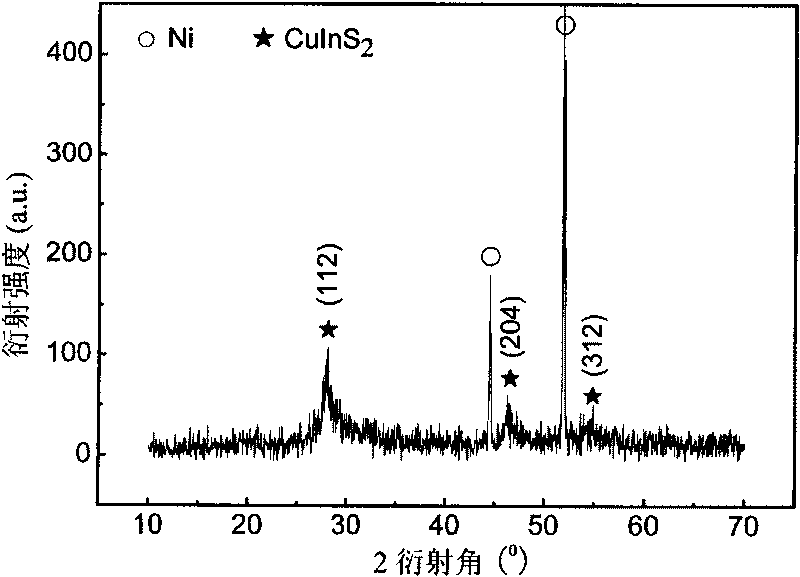
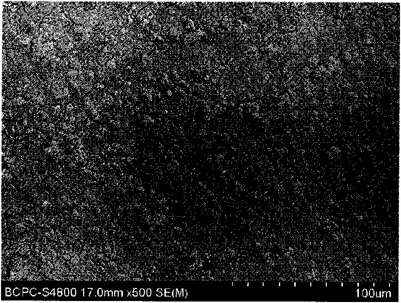
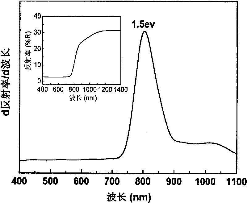
Preparation method of CuInS2 nanometer crystal semiconductor film

A semiconductor and nanocrystalline technology, which is applied in the field of preparation of CuInS2 nanocrystalline semiconductor thin films, can solve problems such as white turbidity, reduced stability, and poor stability of electrodeposition liquid systems, and achieve uniform and stable growth, precise control of film thickness, and enhanced reliability. The effect of controllability and repeatability

Active Publication Date: 2010-06-23
BEIJING UNIV OF CHEM TECH
View PDF0 Cites 19 Cited by
  • Summary
  • Abstract
  • Description
  • Claims
  • Application Information

AI Technical Summary

Problems solved by technology

2) The stability of the electrodeposition solution system is poor
However, under acidic conditions, if the sulfur source concentration is too high, sulfur colloidal particles are easily precipitated in the electrodeposition solution, and white turbidity occurs, which means that its stability is reduced, which is a taboo in the electrodeposition process.

Method used


Image

  • Preparation method of CuInS2 nanometer crystal semiconductor film
  • Preparation method of CuInS2 nanometer crystal semiconductor film
  • Preparation method of CuInS2 nanometer crystal semiconductor film

Examples


Embodiment 1

[0021] 1) Weigh 0.704gC in turn 8 h 5 KO 4 , 0.32gCuCl 2 2H 2 O, 0.44gInCl 3 4H 2 O, 1.49gNa2 S 2 o 3 ·5H 2 O, 0.90g LiCl·H 2 O was dissolved in 150ml deionized water (the reagents used were all analytically pure, and the molar ratio was 2.3:1.25:1:4:10), and the pH of the solution was adjusted to 2.5 with 1mol / l hydrochloric acid, and stirred evenly;

[0022] 2) The solution prepared in step 1) is used as the electrodeposition solution, the pretreated nickel foil is used as the working electrode, the platinum sheet is used as the auxiliary electrode, and saturated calomel is used as the reference electrode, and the three are connected to a constant current electrode with a wire. On the working electrode, auxiliary electrode and reference electrode terminal button of the potentiometer, ensure that the distance between the nickel foil and the platinum sheet is 5cm, and use the temperature control device to control the temperature of the electrodeposition solution at 30...

Embodiment 2

[0026] 1) Weigh 1.056gC in turn 8 h 5 KO 4 , 0.48gCuCl 2 2H 2 O, 0.66gInCl 3 4H 2 O, 2.235gNa 2 S 2 o 3 ·5H 2 O, 1.35g LiCl·H 2 O was dissolved in 200ml of deionized water (the reagents used were all analytically pure, and the molar ratio was 2.3:1.25:1:4:10), and the pH of the solution was adjusted to 2.0 with 1mol / 1 hydrochloric acid, and stirred evenly;

[0027] 2) With the solution prepared in step 1) as the electrodeposition solution, with the pretreated ITO conductive glass as the working electrode, with the platinum sheet as the auxiliary electrode, with saturated calomel as the reference electrode, and connect the three to the On the working electrode, auxiliary electrode and reference electrode terminal buttons of the potentiostat, ensure that the distance between the nickel foil and the platinum sheet is 5cm, and use the temperature control device to control the temperature of the electrodeposition solution at 20±1°C and the potential at -0.95 V(vs.SCE), p...


PUM

PropertyMeasurementUnit
The average particle sizeaaaaaaaaaa
Bandgapaaaaaaaaaa
The average particle sizeaaaaaaaaaa

Abstract

The invention belongs to the field of energy source materials. A preparation method of a CuInS2 nanometer crystal semiconductor film comprises the following steps of: preparing electrodeposit liquid by using copper chloride, indium chloride, sodium thiosulfate and lithium chloride as sources of copper, indium and sulfur and supporting electrolyte, and using potassium acid phthalate as both a complexing agent and a pH buffer; adjusting the pH to 1.5-3.5; carrying out electrodeposition under stirring to obtain a precursor film; and keeping the precursor film at a constant temperature of 250-500DEG C for 30-180 min under the protection of inert atmosphere to obtain the CuInS2 nanometer crystal semiconductor film. The method has strong controllability and good repeatability, and the preparedCuInS2 nanometer crystal semiconductor film contains no impurities and is suitable for the material of the light absorption layer of a thin-film solar cell.

Description

technical field [0001] The invention belongs to the field of energy materials, in particular to CuInS used as a light absorption layer material for solar cells 2 A method for preparing a nanocrystalline semiconductor thin film. Background technique [0002] At present, the serious situation of shortage of conventional fossil fuels and deterioration of the ecological environment has made mankind realize that it is necessary to gradually change the energy consumption structure in the future and vigorously develop clean and renewable energy represented by solar energy. As one of the ideal photovoltaic devices that can effectively utilize solar energy resources, compound thin-film solar cells have the advantages of less consumables, low cost, rich material selection, strong designability, and high theoretical photoelectric conversion efficiency compared with commercialized bulk silicon-based solar cells. Therefore, it is favored by the majority of scientific and technological w...

Claims


Application Information

Patent Timeline
IPC IPC(8): B82B3/00H01L31/18C03C17/22C25D9/04
CPCY02P70/50
Inventor 王峰徐新花吉静刘景军
Owner BEIJING UNIV OF CHEM TECH
Why Eureka
Try Eureka