
Method for preparing hundred nano grade narrow line width holographic grating photoresist pattern with various features

A holographic grating and photoresist technology, which is applied to microlithography exposure equipment, photolithographic process of pattern surface, diffraction grating and other directions, can solve the problems of long electron beam exposure time and high cost, and achieves long time consumption and low cost. Effect

Active Publication Date: 2010-06-16
INST OF SEMICONDUCTORS - CHINESE ACAD OF SCI
View PDF0 Cites 9 Cited by
  • Summary
  • Abstract
  • Description
  • Claims
  • Application Information

AI Technical Summary

Problems solved by technology

Even if it is a 2-stage grating, its period is very small, and it cannot be obtained by ordinary lithography using a general lithography machine. However, a rectangular-period grating can be prepared by electron beam exposure, and a first-stage grating can also be prepared. , the bar width of the grating can be achieved below 50nm, but the exposure time of the electron beam is longer and the cost is higher, while the holographic exposure has the characteristics of low cost and a large area of ​​uniform exposure. In the production of periodic gratings, Advantages over e-beam

Method used


Image

  • Method for preparing hundred nano grade narrow line width holographic grating photoresist pattern with various features
  • Method for preparing hundred nano grade narrow line width holographic grating photoresist pattern with various features
  • Method for preparing hundred nano grade narrow line width holographic grating photoresist pattern with various features

Examples


Embodiment Construction

[0040] In order to make the object, technical solution and advantages of the present invention clearer, the present invention will be described in further detail below in conjunction with specific embodiments and with reference to the accompanying drawings.

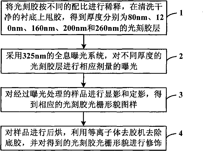
[0041] Such as figure 1 as shown, figure 1 It is a flow chart of a method for preparing a holographic grating photoresist pattern with a narrow line width of a hundred nanometers and various shapes provided by the present invention, and the method includes:

[0042] Step 1: Dilute the photoresist according to different proportions, and shake the glue on the cleaned substrate to obtain photoresist layers with thicknesses of 80nm, 120nm, 160nm, 200nm and 260nm;

[0043] Step 2: Use a 325nm holographic exposure system to expose photoresist layers with different thicknesses in corresponding doses;

[0044] Step 3: developing and fixing the exposed sample to obtain the corresponding photoresist grating pattern;

[0045] Ste...


PUM

PropertyMeasurementUnit
thicknessaaaaaaaaaa
thicknessaaaaaaaaaa

Abstract

The invention discloses a method for preparing a hundred nano grade narrow line width holographic grating photoresist pattern with various features, which comprises the following steps of: 1. diluting photoresist according to different proportions and throwing the photoresist on a clean substrate to obtain photoresist layers with the respective thicknesses of 80nm, 120nm, 160nm, 200nm and 260nm; 2. carrying out the exposure of corresponding dosage on the photoresist layers with different thicknesses by a holographic exposure system with the thickness of 325nm; 3. carrying out development and photographic fixation on a sample after exposure processing to obtain a corresponding photoresist grating feature pattern; 4. after-baking the sample, removing a primer by a plasma resist removing machine and decorating the obtained photoresist grating feature. By utilizing the invention, the hundred nano grade narrow line width holographic grating photoresist pattern with various features is prepared.

Description

technical field [0001] The invention relates to the technical field of semiconductor lasers, in particular to a method for preparing a photoresist pattern of a holographic grating with a narrow line width of one hundred nanometers and multiple shapes, which is mainly used for devices of distributed feedback lasers (DFB) and distributed Bragg lasers (DBR) In the manufacturing process, the grating has the function of mode selection. In addition, it can also be applied to the preparation of optoelectronic devices that require hundreds of nanoscale gratings. Background technique [0002] DFB or DBR laser has the characteristics of dynamic single longitudinal mode and narrow line width. The wavelength is 1.3μm, and the 1.55μm DFB laser is mainly used in optical fiber communication, while the 852.3nm DFB laser is used in the pumping of cesium atomic clocks. [0003] The invention is accomplished under the subject of developing a 852.3nm high-power narrow-linewidth DFB laser. Th...

Claims


Application Information

Patent Timeline
Patent Type & Authority Applications(China)
IPC IPC(8): G02B5/18G03F7/00G03F7/16G03F7/20G03F7/32G03F7/40G03F7/42
Inventor 陈熙钟源陈良惠
Owner INST OF SEMICONDUCTORS - CHINESE ACAD OF SCI
Learn More