N-type nano-diamond film and preparation method
A nano-diamond and thin-film technology, applied in metal material coating process, vacuum evaporation plating, coating, etc., can solve the problems of low carrier mobility, limited application, difficult electronic devices, etc., and achieve high mobility , the method is simple, the effect of low resistivity
- Summary
- Abstract
- Description
- Claims
- Application Information
AI Technical Summary
Problems solved by technology
Method used
Image
Examples
Embodiment 1
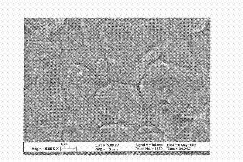
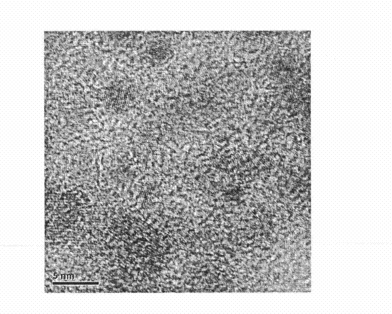
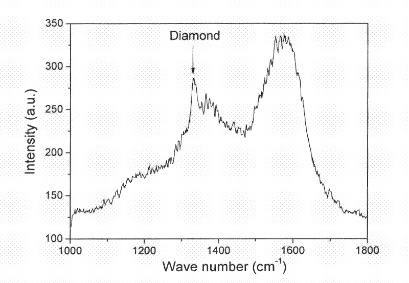
[0030] Polish the monocrystalline silicon wafer with nano-scale diamond powder, and the grinding time is about half an hour. After the polished silicon wafer is cleaned by an ultrasonic machine, it is used as the substrate for the growth of the nano-diamond film. The hot wire chemical vapor deposition method (chemical vapor deposition equipment was purchased from Shanghai Jiaoyou Diamond Coating Co., Ltd.) was used, acetone was used as the carbon source, and acetone was brought into the reaction chamber by hydrogen bubbling. The temperature of the reaction chamber was controlled at 600~ 700° C., the preparation time is 5-6 hours, and a nano-diamond film with a thickness of 3-4 μm is prepared.
[0031] Using a 100keV isotope separator, the implantation energy is 90keV, and the implantation dose in the nano-diamond film is 1015 cm -2 Phosphorus ions and annealed in vacuum at 900 °C for 30 min. The surface of the annealed film was washed with acetone, and then washed with a mix...
Embodiment 2
[0035] The monocrystalline silicon wafer is polished with nanometer diamond powder, and the polishing time is about half an hour. After the polished silicon wafer is cleaned by an ultrasonic machine, it is used as the substrate for the growth of the nano-diamond film. The hot wire chemical vapor deposition method (chemical vapor deposition equipment was purchased from Shanghai Jiaoyou Diamond Coating Co., Ltd.) was used, acetone was used as the carbon source, and acetone was brought into the reaction chamber by hydrogen bubbling. The temperature of the reaction chamber was controlled at 600~ 700° C., the preparation time is 5-6 hours, and a nano-diamond film with a thickness of 3-4 μm is prepared.
[0036] Using a 100keV isotope separator, the implantation energy is 90keV, and the implantation dose in the nano-diamond film is 10 14 cm -2 Oxygen ions (O + , the literature in this field generally uses O + Represents oxygen ions. In the ion implantation process, one electron ...
Embodiment 3
[0040] The monocrystalline silicon wafer is polished with nanometer diamond powder, and the polishing time is about half an hour. After the polished silicon wafer is cleaned by an ultrasonic machine, it is used as the substrate for the growth of the nano-diamond film. The hot wire chemical vapor deposition method (chemical vapor deposition equipment was purchased from Shanghai Jiaoyou Diamond Coating Co., Ltd.) was used, acetone was used as the carbon source, and acetone was brought into the reaction chamber by hydrogen bubbling. The temperature of the reaction chamber was controlled at 600~ 700° C., the preparation time is 5-6 hours, and a nano-diamond film with a thickness of 3-4 μm is prepared.
[0041] Using a 100keV isotope separator, the implantation dose in the nanodiamond film is 10 15 cm -2 Sulfide ion (S + , the literature in this field generally uses S + Indicates sulfur ions. In the ion implantation process, one electron of the atom is generally stripped off to...
PUM
| Property | Measurement | Unit |
|---|---|---|
| thickness | aaaaa | aaaaa |
| size | aaaaa | aaaaa |
| diameter | aaaaa | aaaaa |
Abstract
Description
Claims
Application Information
 - R&D
- Intellectual Property
- Life Sciences
- Materials
- Tech Scout
- Unparalleled Data Quality
- Higher Quality Content
- 60% Fewer Hallucinations
Browse by: Latest US Patents, China's latest patents, Technical Efficacy Thesaurus, Application Domain, Technology Topic, Popular Technical Reports.
© 2025 PatSnap. All rights reserved.Legal|Privacy policy|Modern Slavery Act Transparency Statement|Sitemap|About US| Contact US: help@patsnap.com


